Solar cell

a solar cell and solar cell technology, applied in the field of solar cells, can solve the problems of low photoelectric conversion efficiency of conventional solar cells, and generation of electricity, and achieve the effect of low reflectance and higher photoelectric conversion efficiency

Inactive Publication Date: 2013-11-07
SINO AMERICAN SILICON PROD +1
View PDF14 Cites 14 Cited by
  • Summary
  • Abstract
  • Description
  • Claims
  • Application Information

AI Technical Summary

Benefits of technology

[0009]The invention provides a solar cell. The solar cell has lower reflectance and higher photoelectric conversion efficiency.
[0022]Based on the above, in the solar cell of the invention, a seed layer is disposed on the first surface, and nanorods are formed on the seed layer. The seed layer and the nanorods are used as an antireflection structure, so that the reflectance of the solar cell is significantly reduced. As a result, the incident light absorbed by the solar cell of the invention may be effectively increased, which improves the photoelectric conversion efficiency.

Problems solved by technology

However, the thickness of the conventional single-layer ARC thin film is one quarter of the incident wavelength, and thus the ARC thin film may produce a low reflectance only in a specific range of incident wavelength.
Moreover, because the sunlight incident on the solar cell is generally not at normal incidence, the conventional ARC thin film can not maintain a low reflectance.
Therefore, the conventional silicon-based solar cells that use silicon nitride (SiNx) as single-layer ARC thin films may only generate electricity about 3.5 hours before and after midday.
As a result, the photoelectric conversion efficiency of the conventional solar cell 10 is not high.

Method used


Image

  • Solar cell
  • Solar cell
  • Solar cell

Examples


experimental example 1

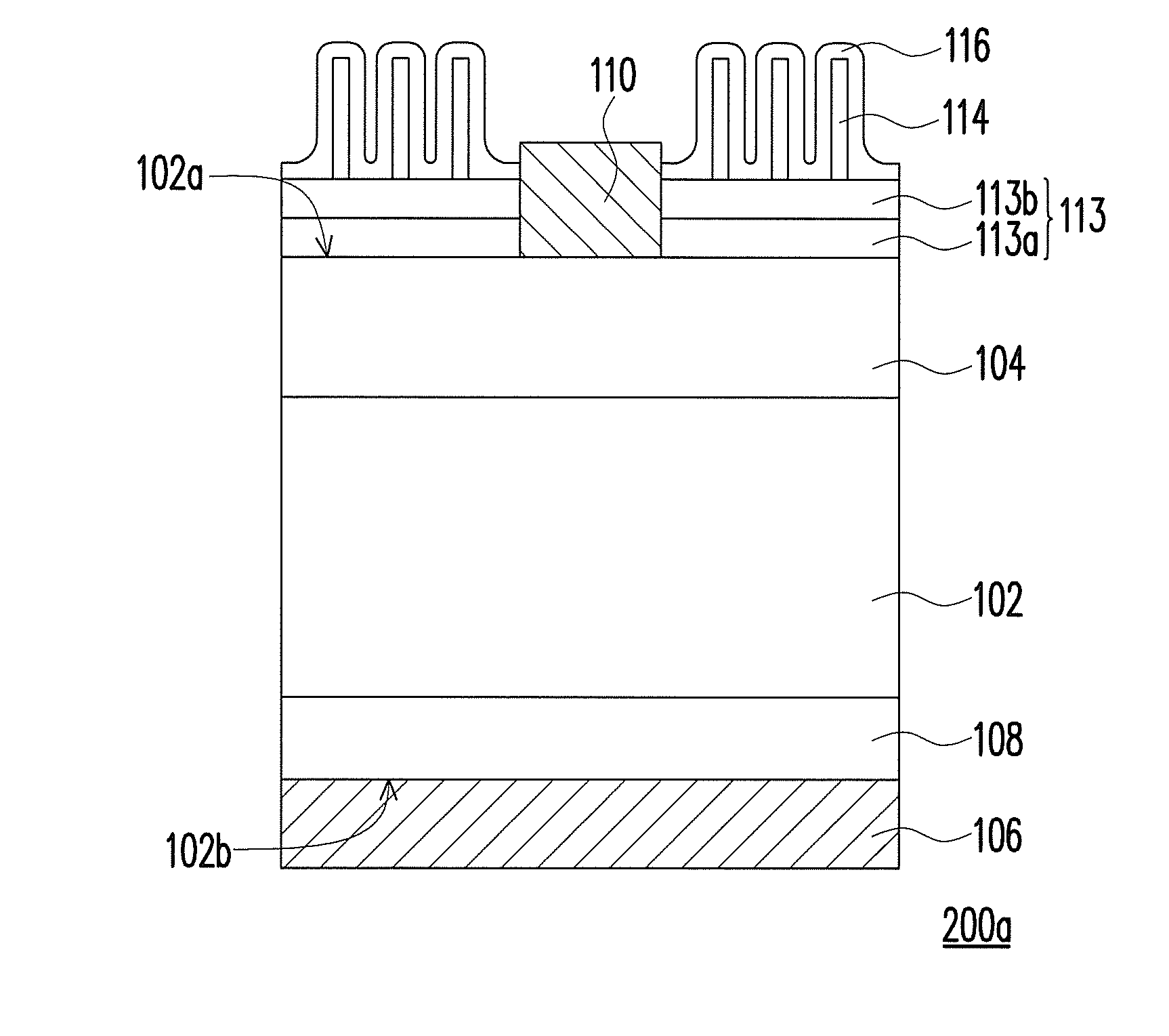
[0048]A phosphorus diffusion process is performed in step 1. Using a p-type silicon wafer as a substrate, the native oxide layer on the silicon wafer is first removed using BOE (buffer oxide etchants, an aqueous solution containing 30% NH4F and 6% HF) solution. Then, a phosphorus pentoxide (P2O5) solution having an 8% weight concentration is spin coated on the p-type silicon wafer. The spin coating includes two stages. The spinning condition at the first stage is 1,500 rpm for 15 seconds, and the spinning condition at the first stage is 2,500 rpm for 35 seconds, wherein the rate and time of the spin coating determine the thickness and uniformity of the phosphorus pentoxide thin film.

[0049]Then, after the spin coating, the silicon wafer is put on a hot plate and heated at 150° C. for 10 minutes, followed by heating at an increased temperature of 200° C. for another 10 minutes. The stability of the thin film containing phosphorus pentoxide is improved by the thermal treatment.

[0050]Th...

experimental example 2

[0061]The seed layer of the solar cell of experimental example 2 is composed of a magnesium oxide buffer layer and a zinc oxide layer, wherein the magnesium oxide buffer layer is first formed on the surface of the substrate, and then the zinc oxide layer is formed on the magnesium oxide buffer layer. Then, a plurality of nanorods are formed on the seed layer to complete a solar cell of experimental example 2.

[0062]FIG. 5 is an X-ray diffraction spectrum of the solar cell of experimental example 1 and experimental example 2, respectively. Curve A of FIG. 5 represents experimental example 1, curve B represents experimental example 2, wherein the peak at about 35° of 20 is the signal from zinc oxide (0002) orientation. Table 2 shows the full width at half maximum (FWHM) of the zinc oxide (0002) peak of the solar cell of experimental example 1 and experimental example 2, respectively.

TABLE 2Full width at halfmaximum (°)Experimental0.41Example 1Experimental0.33Example 2

[0063]Referring to...


PUM


Abstract

A solar cell is provided. The solar cell includes a substrate, a first electrode, a second electrode, a seed layer, and a plurality of nanorods. The substrate has a first surface and a second surface opposite to each other. A conductive type of a portion of the substrate adjacent to the first surface is first conductive type, and a conductive type of the remaining portion of the substrate is second conductive type. The first electrode is disposed on the first surface. The second electrode is disposed on the second surface. The seed layer is disposed on the first surface. The nanorods are disposed on the seed layer.

Description

CROSS-REFERENCE TO RELATED APPLICATION[0001]This application claims the priority benefit of Taiwan application serial no. 101112462, filed on Apr. 9, 2012. The entirety of the above-mentioned patent application is hereby incorporated by reference herein and made a part of this specification.BACKGROUND OF THE INVENTION[0002]1. Field of the Invention[0003]The invention relates to a solar cell, and more particularly, to a solar cell having lower reflectance toward sunlight.[0004]2. Description of Related Art[0005]The silicon-based solar cells are the most popular solar cells in the industry. The concept of silicon-based solar cells is based on introducing dopants into a high-purity semiconductor material (silicon) in order to form a p-type semiconductor and an n-type semiconductor, and then joining the p-type and n-type semiconductors together. As a result, a p-n junction is formed, in which a built-in electrical field is generated. When sunlight irradiates a semiconductor having a p-n...

Claims


Application Information

Patent Timeline
Patent Type & Authority Applications(United States)
IPC IPC(8): H01L31/0216
CPCH01L31/02168Y02E10/50
Inventor CHEN, MIIN-JANGCHEN, HSIN-JUIWANG, WEI-CHENGHSU, WEN-CHING
Owner SINO AMERICAN SILICON PROD
Why Eureka
Try Eureka