Method for producing a film by cu2znsns4 silar

a technology of cu2znsns and silar, which is applied in the direction of liquid/solution decomposition chemical coating, instruments, transportation and packaging, etc., can solve the problems of difficult to obtain only czts, and it is not possible to achieve uniform films of controlled thickness

Inactive Publication Date: 2013-11-14
AUX ENE ALT COMMISSARIAT A LENERGIE ATOMIQUE
View PDF0 Cites 6 Cited by
  • Summary
  • Abstract
  • Description
  • Claims
  • Application Information

AI Technical Summary

Benefits of technology

[0045]Surprisingly, the method according to the invention forms a satisfactory film of CZTS for ratios of the Cu2+, Sn2+ and Zn2+ cations respectively of 1:0.5:0.5 or preferably 1:1:1. It is preferred that the tin and zinc cations are in equivalent concentrations. The concentration of the copper cation is either equivalent or two times higher. These ratios are very advantageous.
[0046]Only a ratio of 1:1:1 or 1:0.5:0.5 makes it possible to obtain a homogeneous film with a single CZTS phase.
[0050]The solution (Na2S) is very stable in time. The solution pH is on the order of 12. The elevated pH of the anionic solution is not harmful for the substrate. The sodium sulfide does not attack the surface of the substrate, because the S2− anions are adsorbed on the cationic layer formed during the immersion of the substrate in the cationic solution. The cationic layer functions to protect the substrate.
[0053]The duration of immersion of the substrate in the cationic solution is advantageously between 15 and 25 seconds. For obtaining a continuous and homogeneous cationic layer, it is not necessary to leave the substrate immersed for a long time. In this way the formation of excessively large particles generating large relief, is avoided. Preferably, nanoparticles having a diameter on the order of 5 nm are formed.

Problems solved by technology

However, they have not made it possible to achieve uniform films of controlled thickness.
However, impurities such as ternary and secondary compounds form more readily than CZTS, and it is therefore difficult to obtain only CZTS.

Method used


Image

  • Method for producing a film by cu2znsns4 silar
  • Method for producing a film by cu2znsns4 silar
  • Method for producing a film by cu2znsns4 silar

Examples


examples

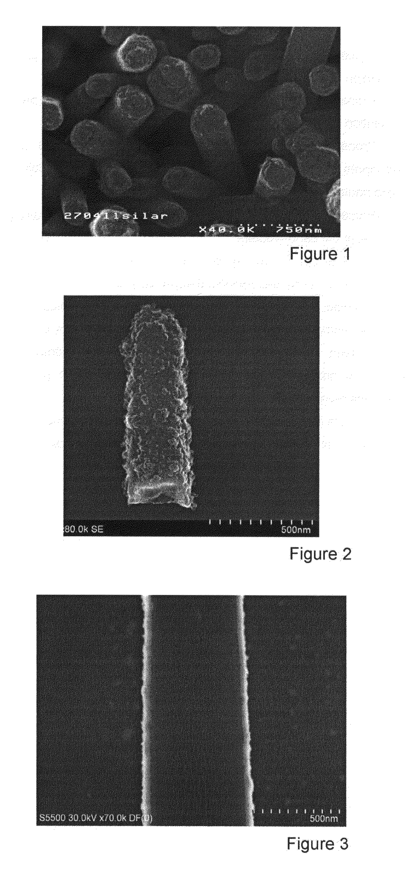
[0058]The method according to the invention was used to form a deposit of CZTS by the SILAR technique on ZnO nanowires. The duration of immersion in the cationic then anionic solutions was 20 seconds each, and the duration of immersion for rinsing in a bath of deionized water was 20 seconds

TABLE 1Description of the different methods used for deposition of CZTSby the SILAR technique.AnionicMethodCationic solutionsolutionP2 5 mM CuSO4 5 mM SnSO410 mM ZnSO410 mM Na2SP310 mM CuSO4 5 mM SnSO410 mM ZnSO410 mM Na2SP410 mM CuSO4 5 mM SnSO4 5 mM ZnSO410 mM Na2SP510 mM CuSO410 mM SnSO410 mM ZnSO410 mM Na2S

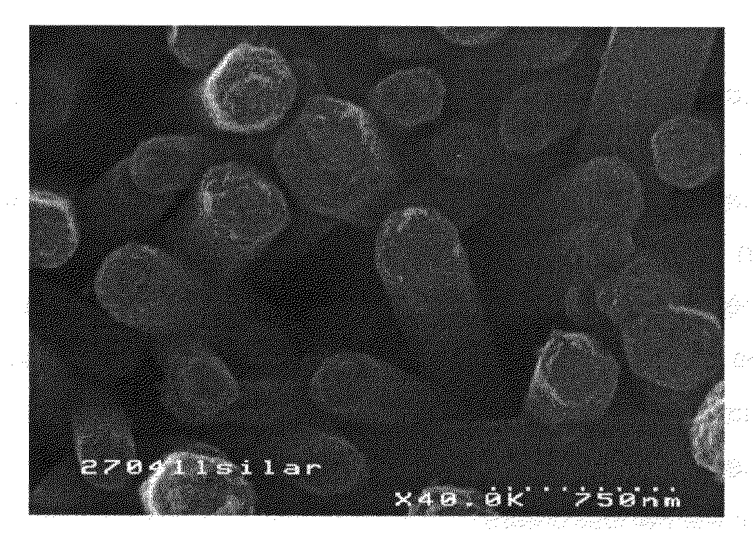
[0059]FIG. 1: SEM image from above of Cu2ZnSnS4 deposited by SILAR on ZnO using method P5.

[0060]FIGS. 2 and 3: STEM image of a structure comprising a ZnO nanowire core and Cu2ZnSnS4 shell using method P5.

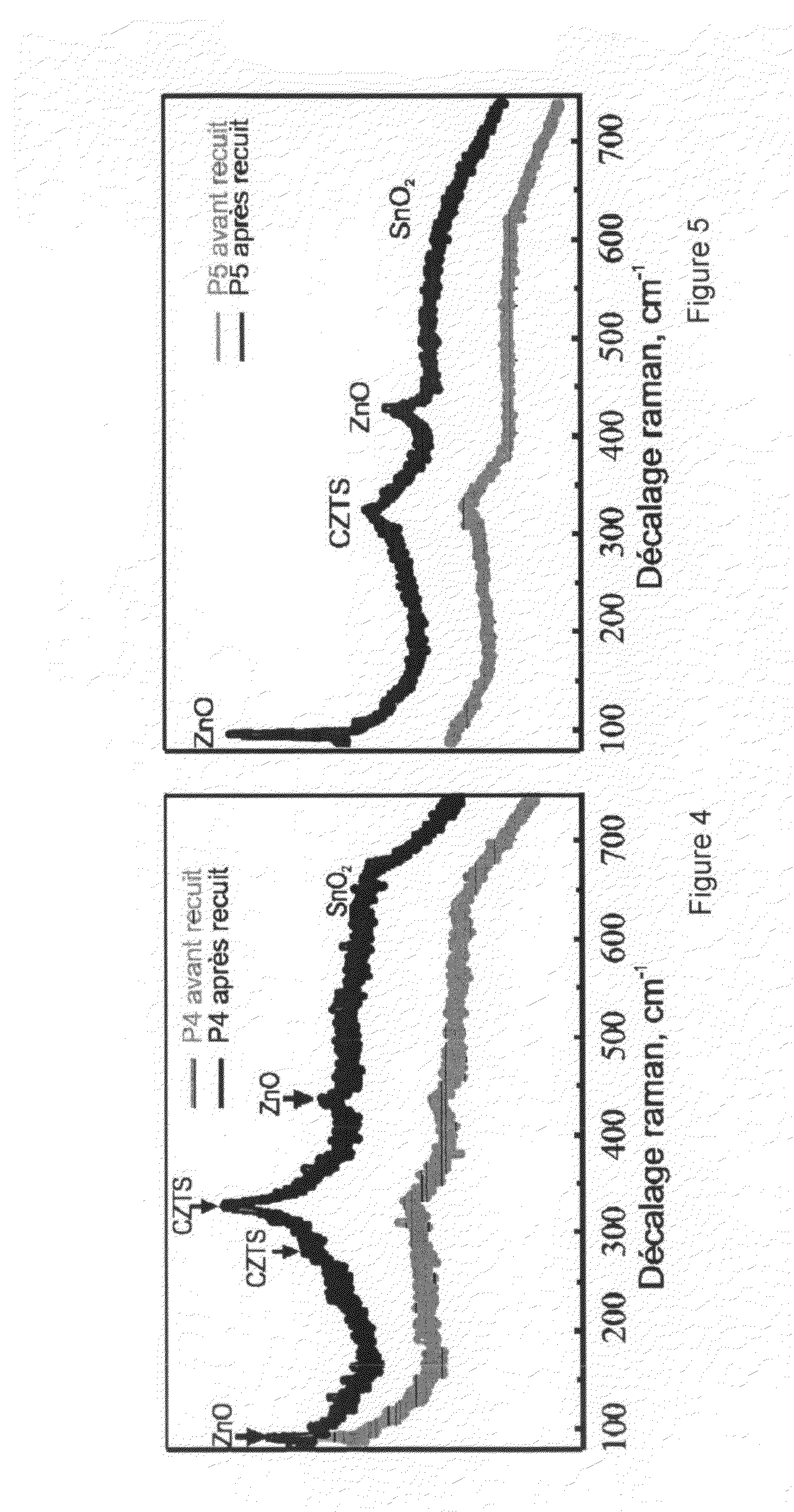
[0061]Analyses by the Raman technique were carried out on the CZTS films obtained by the methods of Table 1.

[0062]FIGS. 4 and 5

[0063]These two spectra correspond to the CZTS films obtained r...


PUM

PropertyMeasurementUnit
pHaaaaaaaaaa
pHaaaaaaaaaa
thicknessaaaaaaaaaa

Abstract

The present invention relates to a method for manufacturing a film of Cu2ZnSnS4 (CZTS) on a metal or metal oxide substrate by successive ion layer adsorption and reaction (SILAR), characterized by the fact that it comprises at least two cycles, each cycle comprising the following successive steps: immersion of the substrate in a cationic solution comprising copper sulfate (CuSO4), tin sulfate (SnSO4) and zinc sulfate (ZnSO4), referred to as the precursors; rinsing by immersion of the substrate in deionized water; immersion of the substrate in an anionic solution comprising sodium sulfide (Na2S); rinsing by immersion of the substrate in deionized water; the concentration ratio of the copper (Cu2+), zinc (Zn2+) and tin (Sn2+) cations and of the sulfur (S2−) anion is 1:1:1:1 or 1:0.5:0.5:1.The invention will be applicable more particularly in the photovoltaic field, especially for production of thin-film, especially nanostructured photovoltaic cells, such as the ETA (Extremely Thin Absorber) cell.

Description

TECHNICAL FIELD[0001]The present invention relates to a method for manufacturing a film of Cu2ZnSnS4, also referred to as CZTS, by adsorption and reaction of successive ionic layers (SILAR in English: Successive Ion Layer Adsorption and Reaction).[0002]This material based on abundant and non-toxic elements has the properties of a semiconductor with a band gap of approximately 1.5 eV. This material is very advantageous for applications in the photovoltaic range, especially for the production of thin-film photovoltaic cells or in particular of nanostructured cells such as the ETA (Extremely Thin Absorber) cell.PRIOR ART[0003]Chemical or electrochemical deposition techniques, such as electrodeposition, spray pyrolysis or chemical bath, have been used. However, they have not made it possible to achieve uniform films of controlled thickness.[0004]CZTS also is synthesized from chemical reactions in the solid state between zinc sulfide (ZnS), copper sulfide (Cu2S) and tin sulfide (SnS2). H...

Claims


Application Information

Patent Timeline
Patent Type & Authority Applications(United States)
IPC IPC(8): C23C2/26
CPCC23C2/26C23C26/00H01L31/0326Y02E10/50B82Y30/00B82Y40/00C23C18/1204C23C18/1245C23C18/125C23C18/1275Y10T428/2958Y10T428/265
Inventor SANCHEZ, SYLVIAIVANOVA-HRISTOVA, VALENTINA
Owner AUX ENE ALT COMMISSARIAT A LENERGIE ATOMIQUE
Why Eureka
Try Eureka