Electric connecting structure comprising preferred oriented Cu6Sn5 grains and method for fabricating the same

a technology of electric connecting structure and oriented cu6sn5 grains, which is applied in the direction of manufacturing tools, transportation and packaging, and manufacturing apparatus, etc., can solve the problems of increasing the manufacturing cost of electronic devices and reducing reliability, so as to improve electrical performance and reliability, eliminate electrical and mechanical property differences in electric connecting structure, and ensure the reliability and lifetime of the joints in the electric connecting structure

Active Publication Date: 2013-11-14
NAT CHIAO TUNG UNIV
View PDF0 Cites 21 Cited by
  • Summary
  • Abstract
  • Description
  • Claims
  • Application Information

AI Technical Summary

Benefits of technology

[0013]In the method for fabricating the electric connecting structure of the present invention, the growth direction of the Cu6Sn5 grains can be well controlled. Hence, the property of microbumps formed by the Cu6Sn5 grains is closed to each other, and preferably identical to each other. Therefore, uniform electrical property among every joint can be obtained, so the electrical performance of the whole electric connecting structure can be further improved.
[0014]In the method for fabricating the electric connecting structure of the present invention, the problem that the conventional solder joints may happen due to the difference crystal orientation of Sn grains can be solved by controlling the growth direction of the Cu6Sn5 grains. When the electric connecting structure of the present invention is applied to flip-chip solder joint structure and three-dimensional integrated circuit (3D-IC) packaging and through silica via (TSV), the property of the solder joints can be ensured. In addition, the method for fabricating the electric connecting structure of the present invention can not only control the mechanical property, the electrical property, the reliability and the lifetime of the joints, but also reduce the manufacturing cost, because that there are no additional barrier materials or high-temperature heating treatment used in the method of the present invention.
[0018]In the step (D) of the method for fabricating the electric connecting structure of the present invention, the reflow process preferably is performed for 30 sec to 10 min. The size and the height of the Cu6Sn5 grains are increased as the reflow time is prolonged.
[0020]In the method for fabricating the electric connecting structure of the present invention, a Cu3Sn layer may be further comprised between the plural Cu6Sn5 grains and the first nano-twinned copper layer, and a ratio between a thickness of the Cu3Sn layer and a maximum height of the Cu6Sn5 grains is represented by: [thickness of the Cu3Sn layer] / [maximum height of the Cu6Sn5 grains], which preferably is 0 to 0.5 and more preferably 1×10⁻⁴ to 0.3. As the storing time of the electric connecting structure is increased, the thickness of the Cu3Sn layer is also extended.
[0031]In the electric connecting structure of the present invention, the growth direction of the Cu6Sn5 grains is well controlled to obtain preferred oriented Cu6Sn5 grains. Hence, the problem that the conventional solder joints may be broken due to the difference crystal orientation of Sn grains can be solved. When the electric connecting structure of the present invention is applied to 3D-IC packaging and through silica via (TSV), the property of the solder joints can be ensured. More specifically, since the growth direction of the Cu6Sn5 grains is well controlled, the property of microbumps formed by the Cu6Sn5 grains is closed to each other, and preferably identical to each other. Therefore, the electrical and mechanical property differences in the electric connecting structure can be eliminated, so the electrical performance and reliability thereof can further be improved.
[0032]In addition, the mechanical property, the electrical property, the reliability and the lifetime of the joints in the electric connecting structure of the present invention can be controlled, and the manufacturing cost thereof can also be reduced, since there are no additional barrier materials or high-temperature heating treatment used in the present invention.

Problems solved by technology

However, the barrier layer causes the manufacturing cost of the electronic device increased, and the reliability thereof may be reduced.

Method used


Image

  • Electric connecting structure comprising preferred oriented Cu6Sn5 grains and method for fabricating the same
  • Electric connecting structure comprising preferred oriented Cu6Sn5 grains and method for fabricating the same
  • Electric connecting structure comprising preferred oriented Cu6Sn5 grains and method for fabricating the same

Examples


embodiment 1

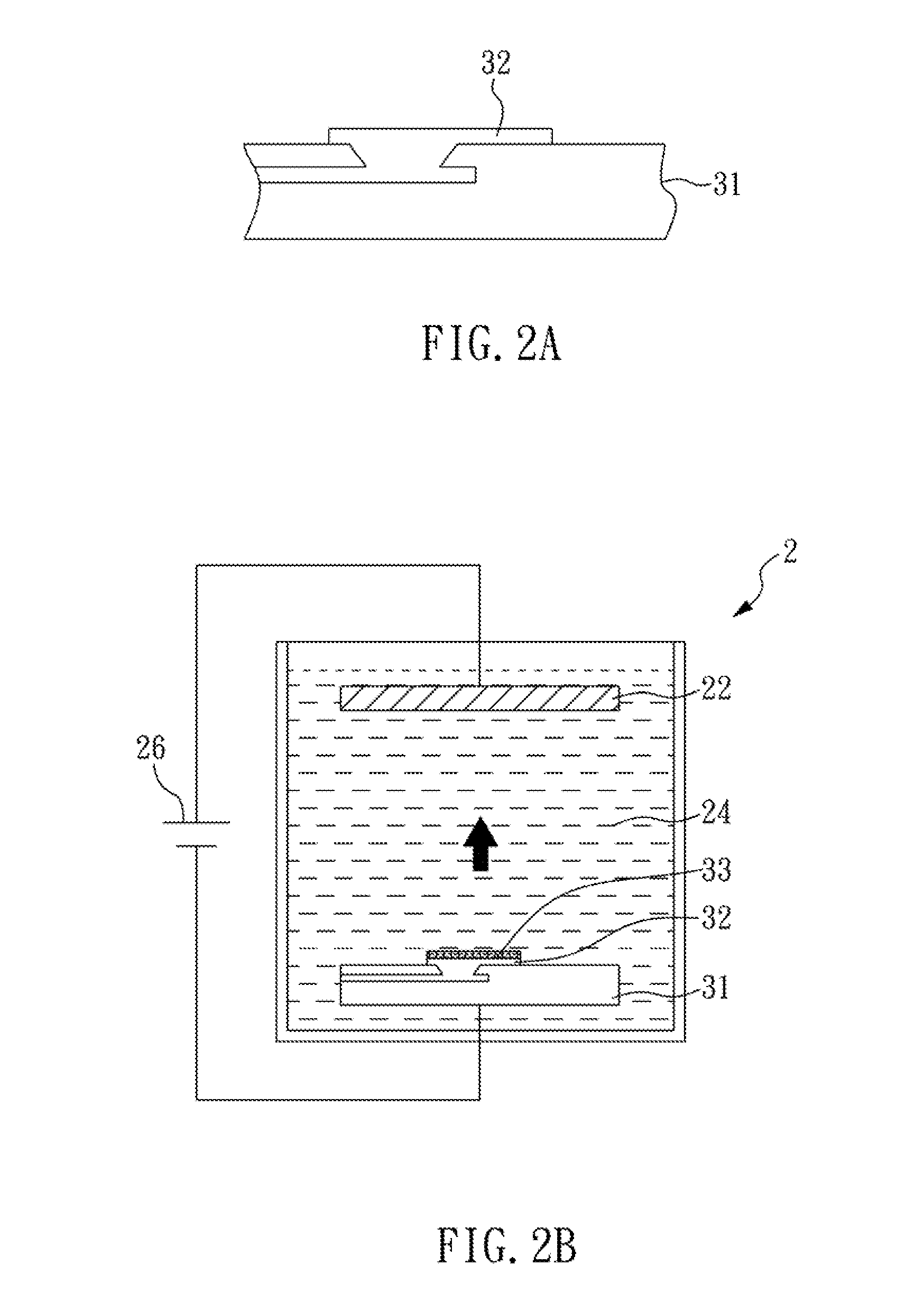
[0055]FIGS. 2A to 2D show a process for fabricating an electric connecting structure according to Embodiment 1 of the present invention. As shown in FIG. 2A, a substrate 31 is provided. In the present embodiment, the substrate 31 is a circuit board with a circuit layer 32 (which can also be used as an electrical pad). Next, as shown in FIG. 2B, the substrate 31 is placed into an electroplating device 2 to use as a cathode. The electroplating device 2 comprises an anode 22, which is immersed in an electroplating solution 24 and electrically connects to a direct current power supply source 26 (Keithley 2400 is used herein). The material used in anode 22 can be copper, phosphor bronze or inert anode material such as platinum plating titanium. The electroplating solution 24 comprises copper sulfate (copper ion concentration being 20-60 g / L), chlorine ion (concentration being 10-100 ppm), and methyl sulfonate (concentration being 80-120 g / L), and other surfactants or lattice dresser (e.g...

embodiment 2

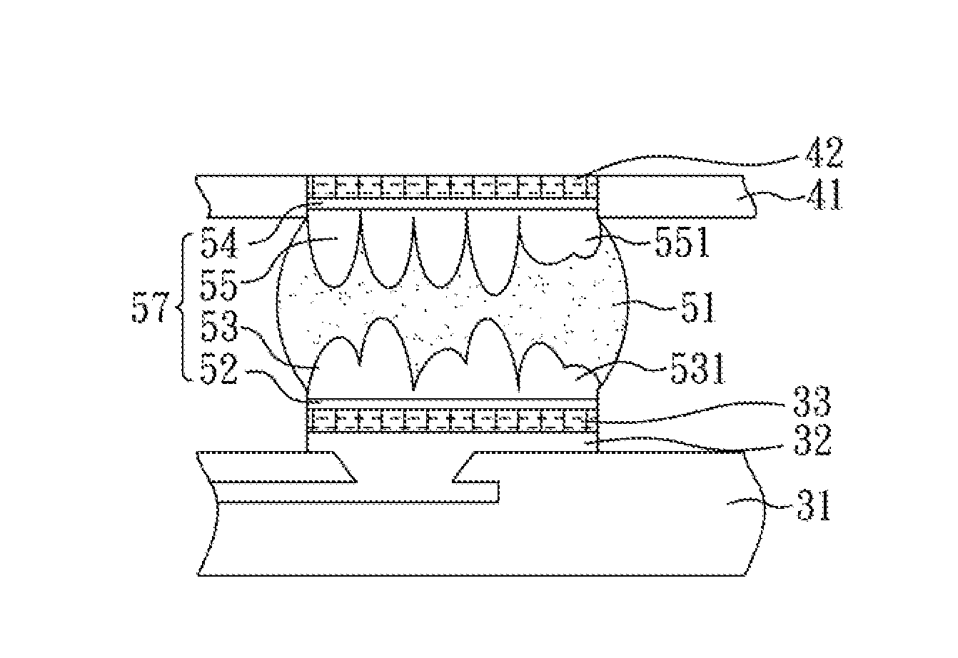
[0063]FIG. 5 is a perspective view showing an electric connecting structure of the present embodiment. The structure and the fabricating method of the electric connecting structure of the present embodiment is similar to that of Embodiment 1, except that the reflow time used in the present embodiment is longer than that used in Embodiment. The reflow time is about 5-6 min, so the size of the Cu6Sn5 grains 551, 531 is increased and the thickness of the Cu6Sn5 layer 55 is increased to about 10 μm-30 μm. In the present embodiment, the thickness of the solder 51 and the reflow time performed thereon are adjusted, so the Cu6Sn5 grains 551, 531 on the surfaces of the substrate 31 and the semiconductor 41 can be adhered to each other. In addition, the inventor confirmed that the Cu6Sn5 grains are still well oriented, even though the Cu6Sn5 grains 551, 531 are adhered to each other. The aforementioned result indicates that the method of the present invention can control the growth direction...


PUM

PropertyMeasurementUnit
thicknessaaaaaaaaaa
thicknessaaaaaaaaaa
temperatureaaaaaaaaaa

Abstract

An electric connecting structure comprising preferred oriented Cu6Sn5 grains and a method for fabricating the same are disclosed. The method of the present invention comprises steps: (A) providing a first substrate; (B) forming a first nano-twinned copper layer on part of a surface of the first substrate; (C) using a solder to connect the first substrate with a second substrate having a second electrical pad, in which the second electrical pad comprises a second nano-twinned copper layer, and the solder locates between the first nano-twinned copper layer and the second nano-twinned copper layer; and (D) reflowing at the temperature of 200° C. to 300° C. to transform at least part of the solder into an intermetallic compound (IMC) layer, in which the IMC layer comprises plural Cu6Sn5 grains with a preferred orientation; wherein at least 50% in volume of the first and second nano-twinned copper layer comprises plural grains.

Description

CROSS REFERENCE TO RELATED APPLICATION[0001]This application claims the benefits of the Taiwan Patent Application Serial Number 101116641, filed on May 10, 2012, the subject matter of which is incorporated herein by reference.BACKGROUND OF THE INVENTION[0002]1. Field of the Invention[0003]The present invention relates to an electric connecting structure and a method for fabricating the same and, more particularly, to an electric connecting structure comprising preferred oriented Cu6Sn5 grains and a method for fabricating the same.[0004]2. Description of Related Art[0005]Copper (Cu) is generally used in metal connecting devices (for examples, metal interconnects, under bump metallizations (UBMs), Cu pillar, or through silicon via (TSV) because of its high electrical conductivity and thermal transferring ability.[0006]For instance, when Cu is applied in the UBM of a packaging structure, UBM is frequently electrically connected to other electronic elements through soldering. The proces...

Claims


Application Information

Patent Timeline
Patent Type & Authority Applications(United States)
IPC IPC(8): H01R13/03H01R43/02
CPCH01R13/03H01R43/02H01L24/11H01L21/4846H01L24/03H01L24/05H01L24/13H01L24/16H01L24/81H01L2224/03462H01L2224/05541H01L2224/05647H01L2224/81191H01L2224/81447H01L2224/8181H01L2224/81815H01L2924/3651H01L2224/16503H01L2224/13111B23K1/0016H01L2224/0401H01L2924/01322Y10T428/12903Y10T29/49213H01L2924/00012H01L2924/01047H01L2924/01029H01L2924/00014H01L2924/00
Inventor CHEN, CHIHLIN, HAN-WEN
Owner NAT CHIAO TUNG UNIV
Why Eureka
Try Eureka