Semiconductor device and method for manufacturing the same

a technology of semiconductors and semiconductors, applied in the direction of semiconductor devices, electrical devices, transistors, etc., can solve the problems of difficult to obtain transistor characteristics, and achieve the effect of high field-effect mobility

Inactive Publication Date: 2013-12-05
SEMICON ENERGY LAB CO LTD
View PDF2 Cites 102 Cited by
  • Summary
  • Abstract
  • Description
  • Claims
  • Application Information

AI Technical Summary

Benefits of technology

[0047]A transistor structure with high field-effect mobility can be achieved.

Problems solved by technology

Further, when a silicon nitride film is used as the insulating film, a large amount of carriers flow in an interface between the silicon nitride film and the oxide semiconductor layer, which makes it difficult to obtain transistor characteristics.

Method used


Image

  • Semiconductor device and method for manufacturing the same
  • Semiconductor device and method for manufacturing the same
  • Semiconductor device and method for manufacturing the same

Examples


embodiment 1

(Embodiment 1)

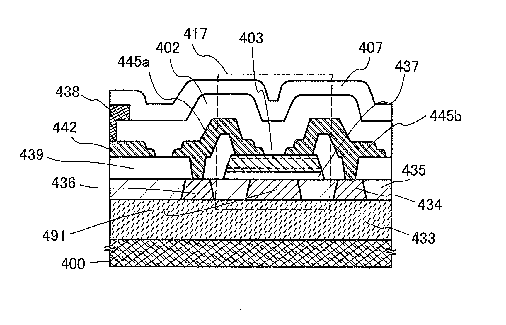
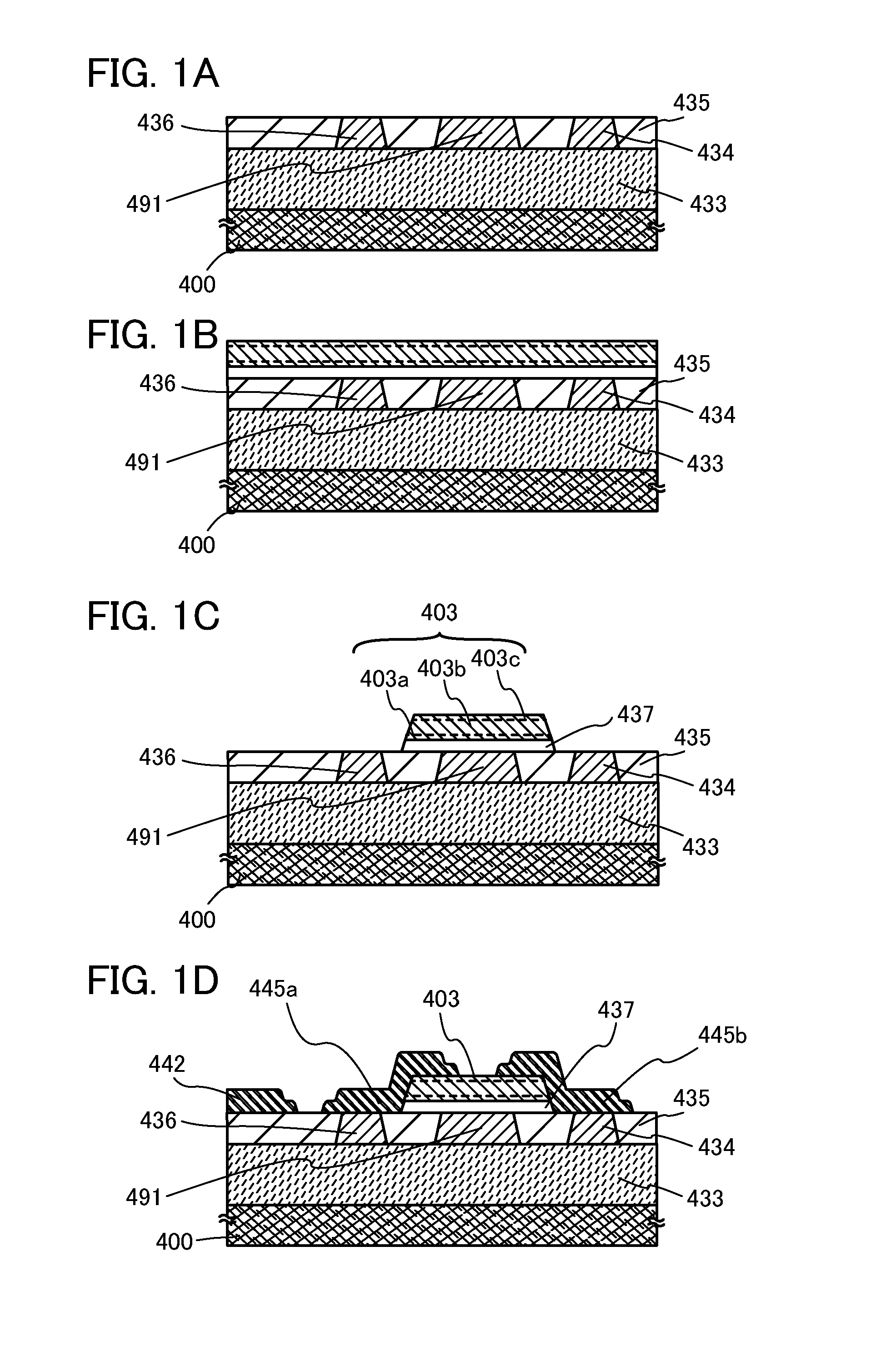
[0059]In this embodiment, one embodiment of a semiconductor device and a method for manufacturing the semiconductor device will be described with reference to FIGS. 1A to 1D. In this embodiment, an example of a method for manufacturing a transistor including an oxide semiconductor film is described.

[0060]First, an insulating film 433 is formed over a substrate 400 having an insulating surface. A conductive film is formed over the insulating film 433 by a sputtering method, an evaporation method, or the like, and the conductive film is etched, so that a conductive layer 491 and wiring layers 434 and 436 are formed.

[0061]There is no particular limitation on a substrate that can be used as the substrate 400 having an insulating surface as long as it has heat resistance high enough to withstand heat treatment performed later. For example, a glass substrate of barium borosilicate glass, aluminoborosilicate glass, or the like, a ceramic substrate, a quartz substrate, or a sa...

embodiment 2

(Embodiment 2)

[0095]In this embodiment, an example of a method for manufacturing a bottom-gate transistor will be described below. Part of steps in a manufacturing process is the same as that in Embodiment 1, and thus the detailed description of the part of the steps is omitted.

[0096]First, steps up to and including the step in FIG. 1C, which are described in Embodiment 1, are performed. Specifically, over the substrate 400, the conductive layer 491 and the wiring layers 434 and 436 are formed. Over the conductive layer 491 and the wiring layers 434 and 436, an oxide insulating film is formed. Then, polishing treatment (CMP) is performed, so that the planarized oxide insulating film 435 is formed and top surfaces of the wiring layers 434 and 436 and a top surface of the conductive layer 491 are exposed. After the CMP treatment, cleaning is performed, and then heat treatment for removing moisture attached on the substrate is performed. After the planarization, the insulating film 437...

embodiment 3

(Embodiment 3)

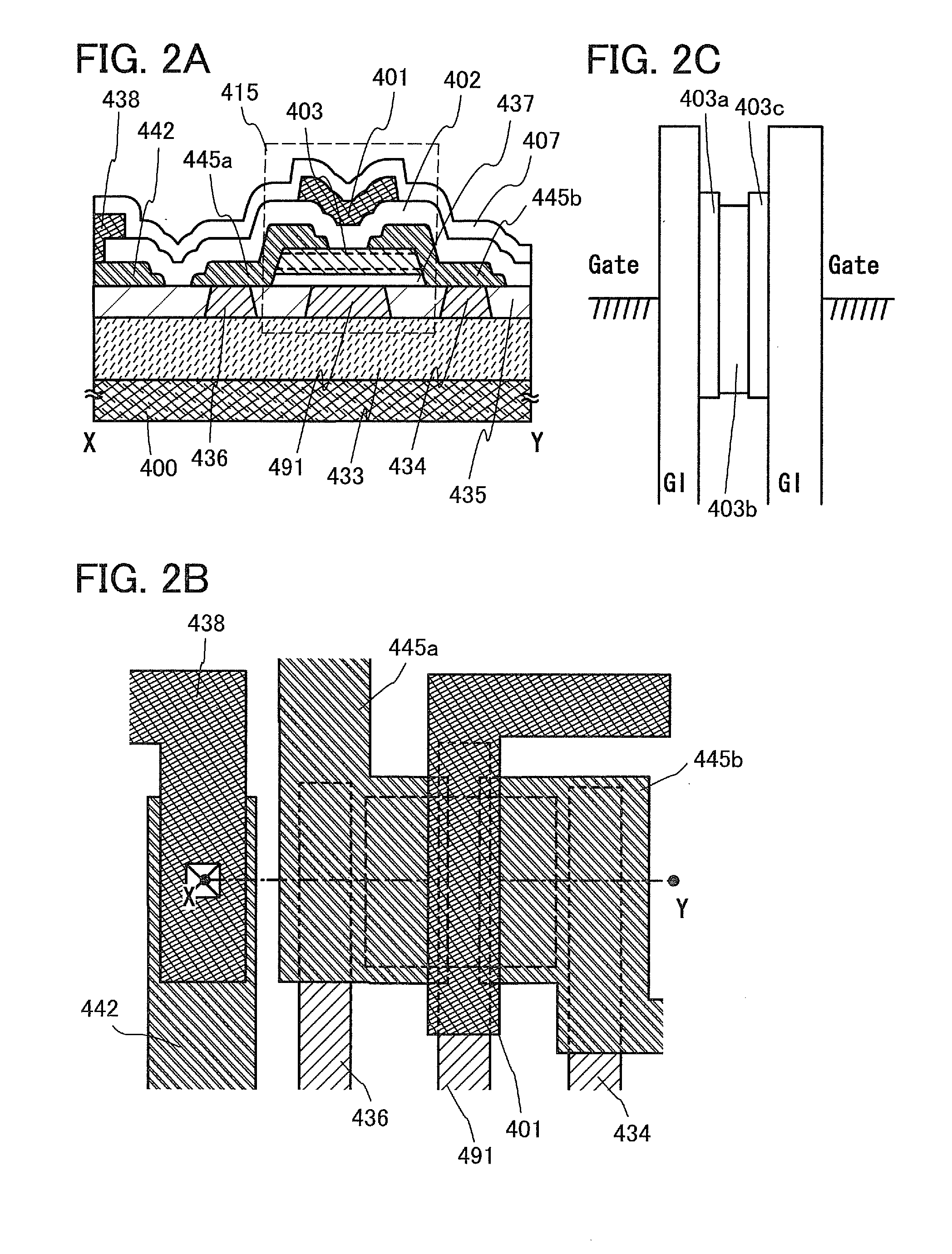
[0105]In this embodiment, an example of a semiconductor device including the transistor described in Embodiment 1 will be described with reference to FIGS. 4A and 4B.

[0106]The semiconductor device illustrated in FIGS. 4A and 4B includes transistors 740 and 750 including a first semiconductor material in a lower portion, and a transistor 610 including a second semiconductor material in an upper portion. The transistor 610 has the same structure as the transistor 415 described in Embodiment 1. The same reference numerals are used for the same parts as those in FIGS. 2A to 2C. FIG. 4B is a circuit diagram of the semiconductor device in FIG. 4A.

[0107]Here, the first semiconductor material and the second semiconductor material are preferably materials having different band gaps. For example, the first semiconductor material may be a semiconductor material other than an oxide semiconductor (e.g., silicon) and the second semiconductor material may be an oxide semiconductor. A...


PUM


Abstract

In order to form a structure in which an oxide semiconductor layer through which a carrier flows is not in contact with a gate insulating film, a buried channel structure in which the oxide semiconductor layer through which a carrier flows is away from the gate insulating film containing silicon is provided. Specifically, a buffer layer is provided between the gate insulating film and the oxide semiconductor layer. Both the oxide semiconductor layer and the buffer layer are formed using materials containing indium and another metal element. The composition of indium with respect to gallium contained in the oxide semiconductor layer is higher than the composition of indium with respect to gallium contained in the buffer layer. The buffer layer has a smaller thickness than the oxide semiconductor layer.

Description

TECHNICAL FIELD[0001]The present invention relates to a semiconductor device including an oxide semiconductor and a manufacturing method thereof.[0002]In this specification, a semiconductor device generally means a device which can function by utilizing semiconductor characteristics, and an electrooptic device, a semiconductor circuit, and electronic equipment are all semiconductor devices.BACKGROUND ART[0003]In recent years, semiconductor devices have been developed to be used mainly for an LSI, a CPU, or a memory. A CPU is an aggregation of semiconductor elements each provided with an electrode which is a connection terminal, which includes a semiconductor integrated circuit (including at least a transistor and a memory) separated from a semiconductor wafer.[0004]A semiconductor circuit (IC chip) of an LSI, a CPU, or a memory is mounted on a circuit board, for example, a printed wiring board, to be used as one of components of a variety of electronic devices.[0005]A technique for ...

Claims


Application Information

Patent Timeline
Patent Type & Authority Applications(United States)
IPC IPC(8): H01L29/786
CPCH01L29/78693H01L29/7869H01L29/78606H01L29/045H01L29/78648
Inventor YAMAZAKI, SHUNPEI
Owner SEMICON ENERGY LAB CO LTD
Why Eureka
Try Eureka