Semiconductor device and manufacturing method thereof

Active Publication Date: 2013-12-12
FUJI ELECTRIC CO LTD
View PDF0 Cites 11 Cited by
  • Summary
  • Abstract
  • Description
  • Claims
  • Application Information

AI Technical Summary

Benefits of technology

[0034]According to the invention, by an uppermost surface semiconductor layer configuring a double-RESURF structure being formed so that high concentration regions with a deep diffusion depth and low concentration regions with a shallow diffusion depth are alternately arranged adjacent to each other, it is possible to increase a lateral resistance without changing the total amount of electric charges in the uppermost surface semiconductor

Problems solved by technology

The double-RESURF structure is suitable for a realization of a high breakdown voltage, but has a problem in that as its junction area is large, a parasitic capacitance is high.
Because of this, malfunction is liable to occur

Method used


Image

  • Semiconductor device and manufacturing method thereof
  • Semiconductor device and manufacturing method thereof
  • Semiconductor device and manufacturing method thereof

Examples


Example

Working Example 1

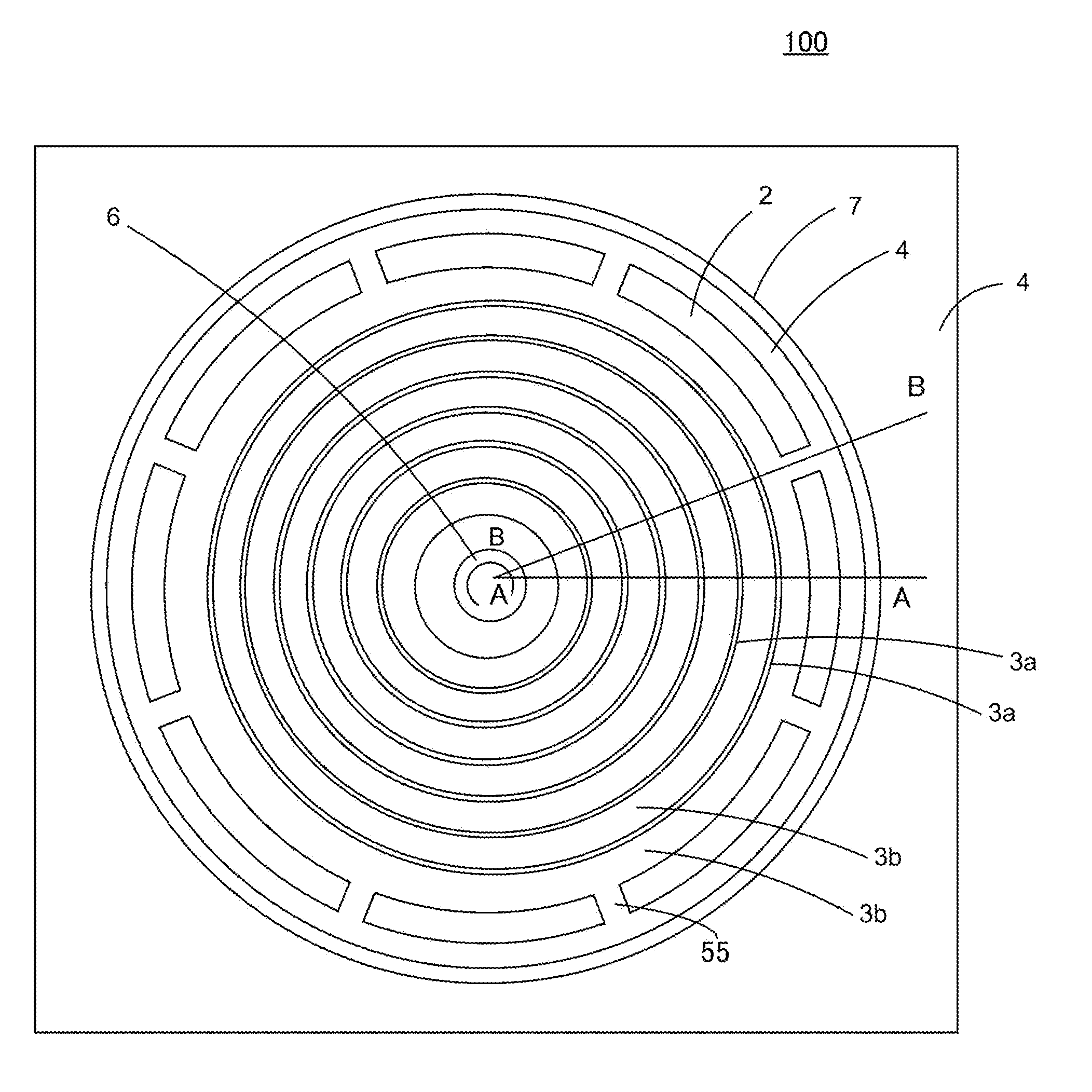
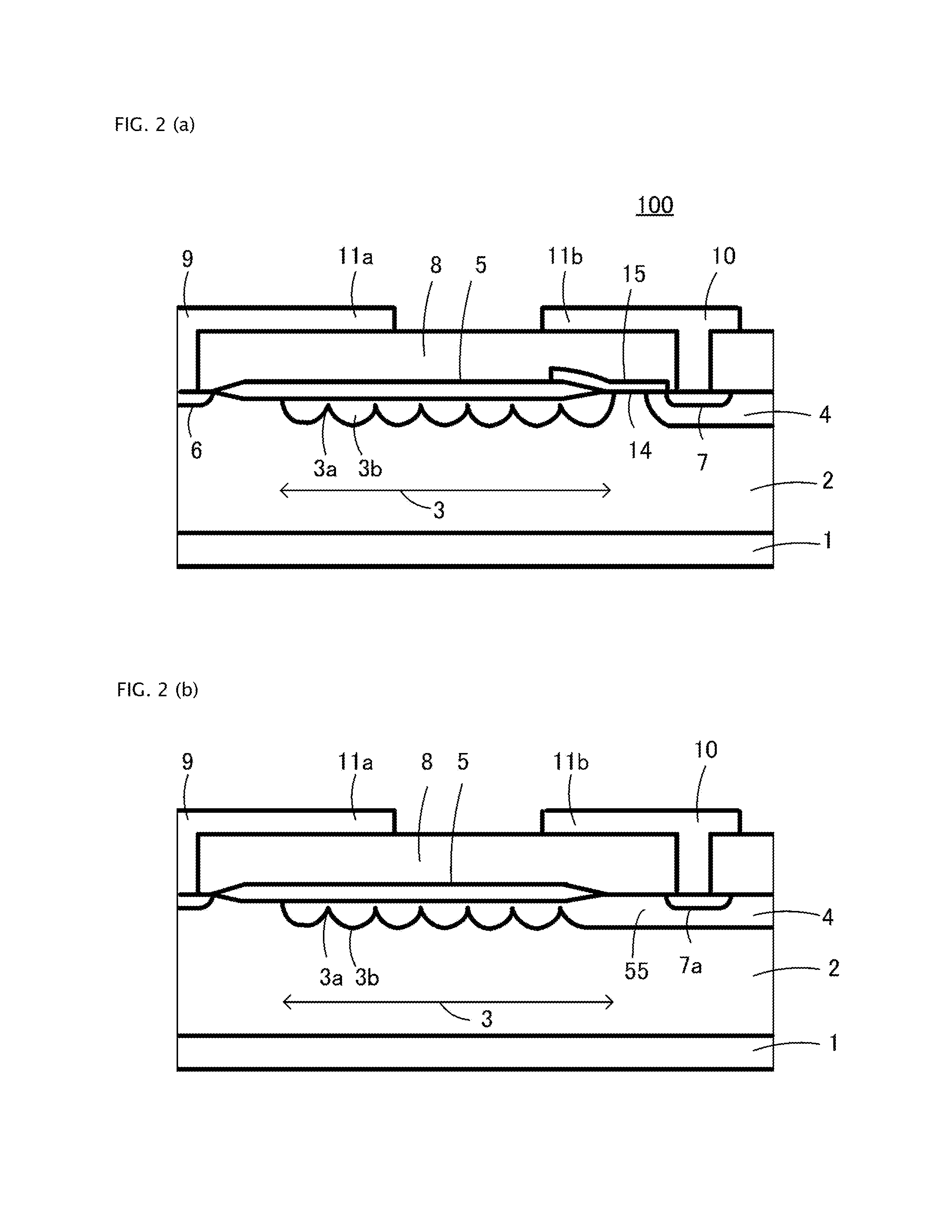
[0058]FIGS. 1 to 2B are configuration diagrams of a semiconductor device according to a first working example of the invention, wherein FIG. 1 is a main portion plan view, FIG. 2A is a main portion sectional view taken along line A-A of FIG. 1, and FIG. 2B is a main portion sectional view taken along line B-B of FIG. 1. FIGS. 1 to 2B show a MOSFET used as a level shifter formed in an HVIC described in FIG. 16 or 18. The MOSFET is formed in a low potential region, and drain electrode 9 is connected to a high potential region by a bonding wire (not shown). Also, the outer peripheral end of p-type well region 4 acting as the low potential region is shown in a circular shape here but, not being limited to this, expands outward to any size.

[0059]Semiconductor device 100 includes n-type semiconductor layer 2 formed on a surface layer of p-type semiconductor substrate 1 and p-type diffusion layer 3 formed on a surface layer of n-type semiconductor layer 2. N-type semicondu...

Example

Working Example 2

[0081]FIGS. 7 to 9B are configuration diagrams of a semiconductor device 200 according to a second working example of the invention, wherein FIG. 7 is a main portion plan view, FIG. 8 is an enlarged main portion plan view of an F portion in FIG. 7, FIG. 9A is a main portion sectional view taken along line C-C of FIG. 8, and FIG. 9B is a main portion sectional view taken along line D-D of FIG. 8.

[0082]In FIG. 7, high voltage isolation structure 20, having an annular zonal shape with a fixed width in a plan view, encloses high potential region 18. The plan-view outline of high voltage isolation structure 20 includes linear portions 16 and corner portions 17 having a curved shape with a fixed curvature. The width of high voltage isolation structure 20 is approximately 200 μm, and the curvature radius of corner portions 17 is approximately 80 μm.

[0083]The difference from semiconductor device 100 of the first working example is that a level shift MOSFET is formed in high...

Example

Working Example 3

[0086]FIGS. 10A to 10C, showing a method of manufacturing a semiconductor device according to a third working example of the invention, are main portion manufacturing process sectional views shown in a process order. Herein, FIGS. 10A to 10C show a process of manufacturing the semiconductor device 200 of the second working example. The manufacturing process sectional views correspond to the sectional view of FIG. 9A. Also, herein, FIGS. 10A to 10C show steps of using a shielding mask to form the p-type low concentration regions 3a and p-type high concentration regions 3b configuring p-type diffusion layer 3.

[0087]Resist mask 21 acting as a shielding mask is formed on a surface of n-type semiconductor layer 2 (FIG. 10A). Next, boron 22 is ion implanted. The dose amount is set to an optimal value (a dose amount wherein a breakdown voltage is highest) satisfying double-RESURF conditions (FIG. 10B).

[0088]After resist mask 21 is removed, a heat treatment is performed to ...


PUM


Abstract

A semiconductor device is disclosed which has a high voltage isolation structure that is a RESURF structure, wherein it is possible to reduce a displacement current generated by dV/dt noise, and a method of manufacturing the semiconductor device. It is possible to increase a lateral resistance without changing the total amount of electric charges in the uppermost surface p-type diffusion layer by using an uppermost surface p-type diffusion layer configuring a double-RESURF structure being formed so that high concentration regions with a deep diffusion depth and low concentration regions with a shallow diffusion depth are alternately arranged adjacent to each other. As a result, it is possible to reduce a displacement current generated by dV/dt noise.

Description

BACKGROUND OF THE INVENTION[0001]A. Field of the Invention[0002]The present invention relates to a semiconductor device such as a high voltage integrated circuit (HVIC) having a high voltage isolation structure that is a double-RESURF structure, and to a method of manufacturing the semiconductor device.[0003]B. Description of the Related Art[0004]In an industrial inverter, heretofore, a transformer or a photocoupler has been used for electrical insulation in order to gate drive a semiconductor device such as an IGBT configuring a power conversion bridge circuit. In recent years, in order to reduce cost a high voltage IC with no electrical insulation has been used mainly for low-power applications.[0005]FIG. 16 is a common gate drive circuit diagram of a high voltage IC. High voltage IC (HVIC) 806 includes high side drive circuit 803 that operates using a power source Vb with an emitter potential (Vs) at the low potential side main terminal of upper arm IGBT 801 as a reference. Also,...

Claims


Application Information

Patent Timeline
IPC IPC(8): H01L29/739H01L29/66
CPCH01L29/7393H01L29/66325H01L21/266H01L29/402H01L29/42368H01L29/66659H01L29/66681H01L29/7816H01L29/7824H01L29/7835H01L29/0634H01L29/0696H01L29/1095
Inventor JONISHI, AKIHIRO
Owner FUJI ELECTRIC CO LTD
Why Eureka
Try Eureka