Method for forming compound epitaxial layer by chemical bonding and epitaxy product made by the same method

a compound epitaxial layer and chemical bonding technology, applied in the direction of crystal growth process, polycrystalline material growth, semiconductor/solid-state device details, etc., can solve the problems of low binding strength of mbe product between epitaxial layers, insufficient high vacuum, and delamination of epitaxial layers, etc., to achieve sufficient binding strength and increase product yield

Inactive Publication Date: 2014-01-09
LIN HUEY JEAN
View PDF5 Cites 1 Cited by
  • Summary
  • Abstract
  • Description
  • Claims
  • Application Information

AI Technical Summary

Benefits of technology

[0009]In view of the various problems of the conventional epitaxy methods, the inventor of the present invention conducted extensive research and experiment and finally succeeded in developing a method for forming a compound epitaxial layer by chemical bonding and an epi...

Problems solved by technology

The low deposition rate, however, also means that a sufficiently high vacuum is required to achieve the same purity level as other deposition methods.
Nevertheless, an MBE product tends to have relatively low binding strength between the epitaxial layers, which are bound together by physical contact.
According to years of research and observation by the inventor of the present invention, a product made by the conventional MBE method is subject to delamination of the epitaxial layers, which is highly un...

Method used


Image

  • Method for forming compound epitaxial layer by chemical bonding and epitaxy product made by the same method
  • Method for forming compound epitaxial layer by chemical bonding and epitaxy product made by the same method
  • Method for forming compound epitaxial layer by chemical bonding and epitaxy product made by the same method

Examples


Embodiment Construction

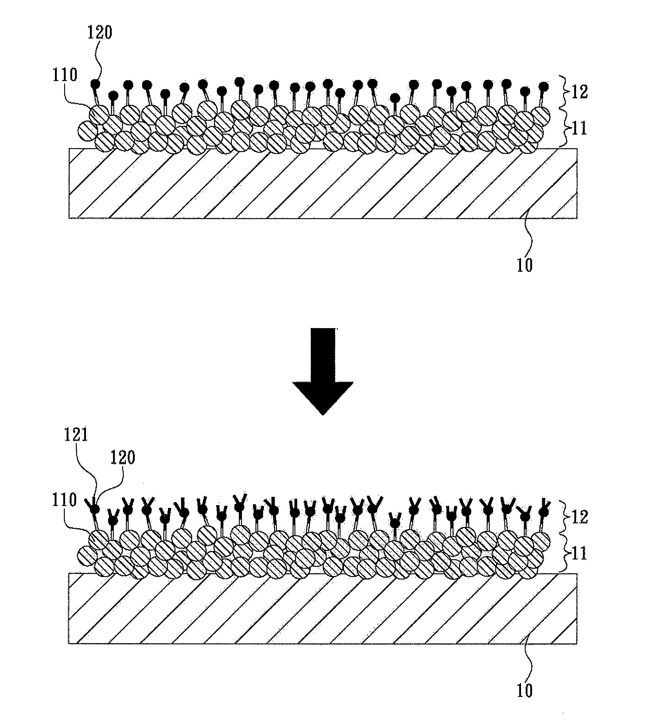
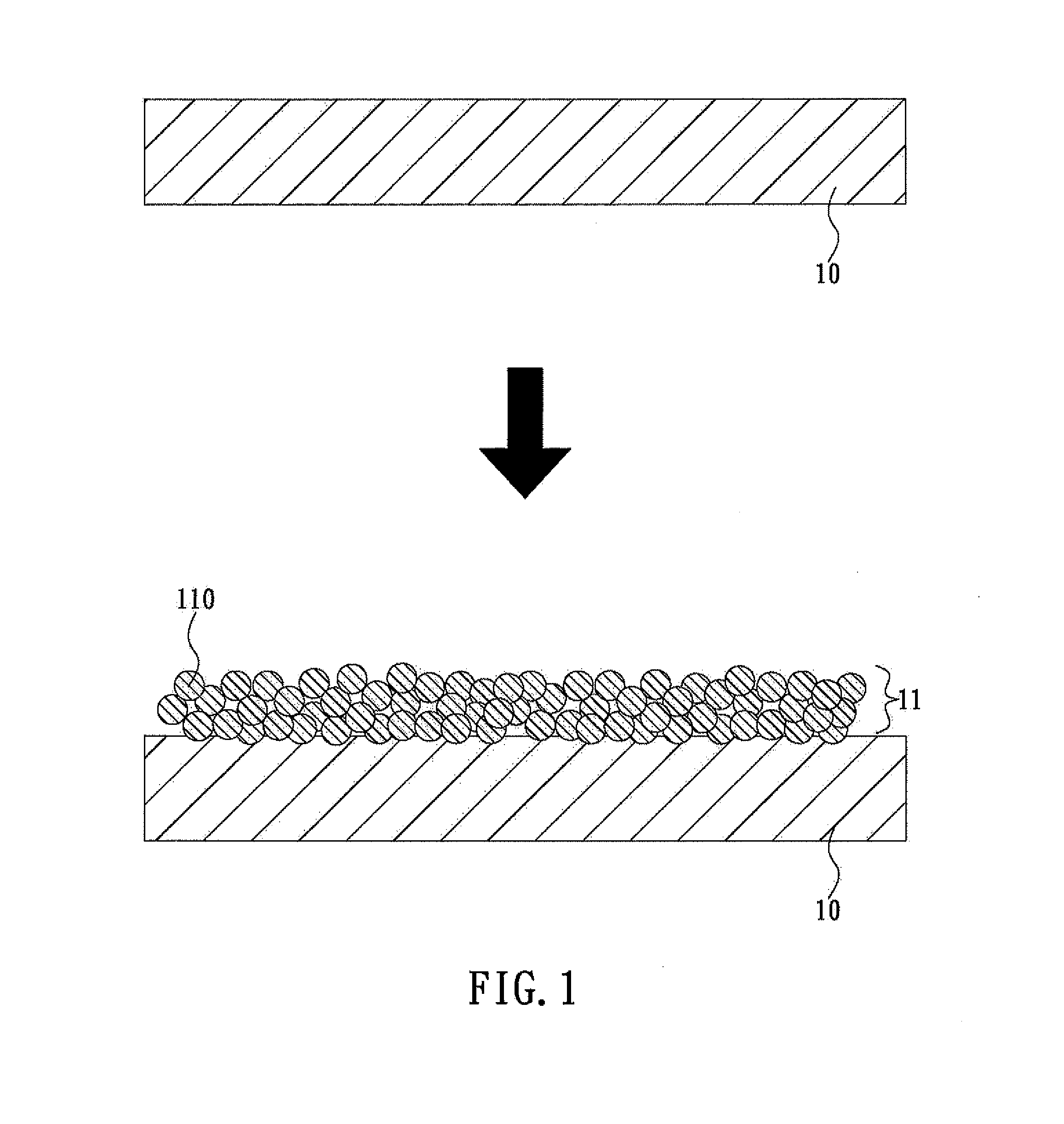
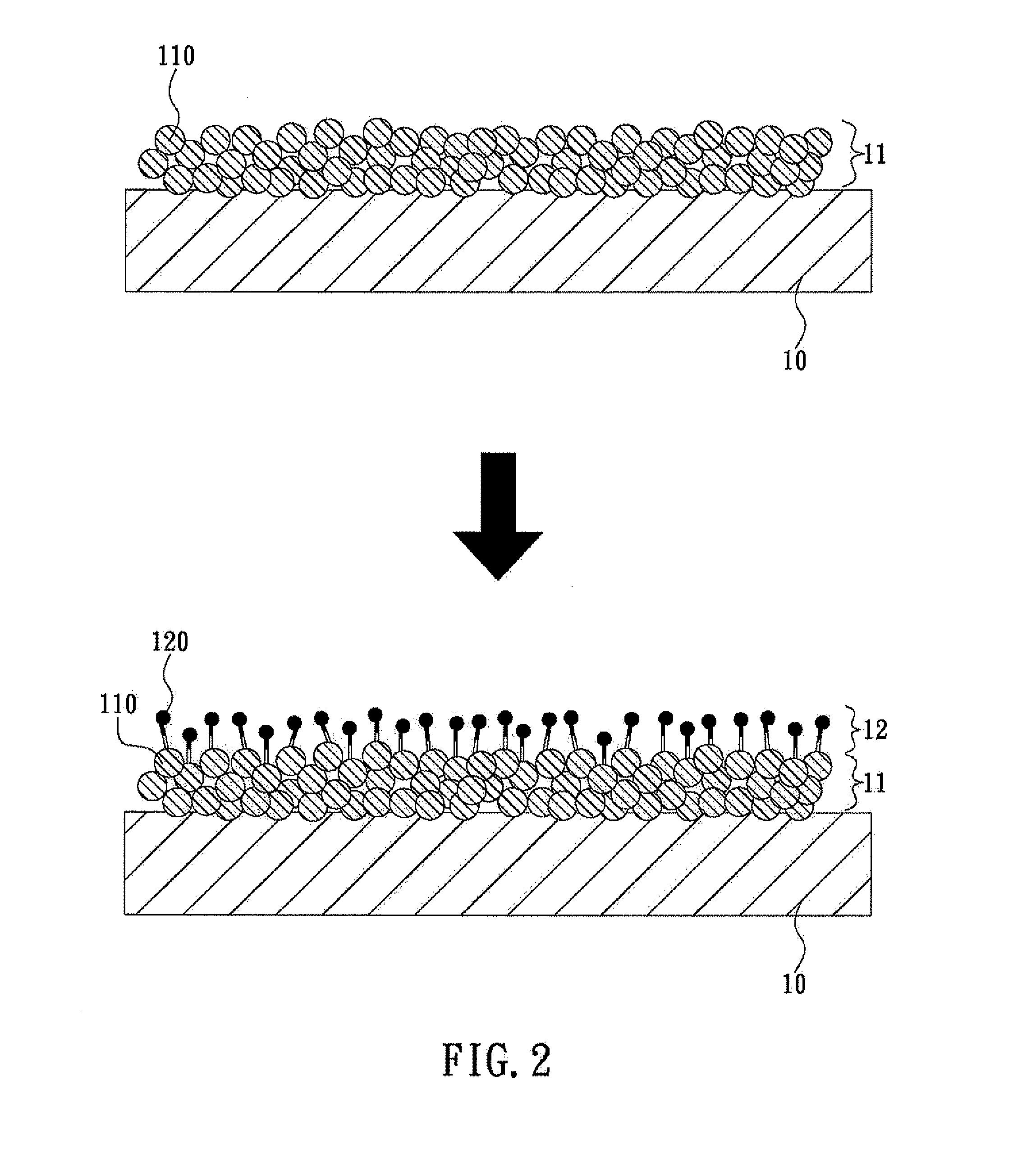
[0022]The inventor of the present invention has long been engaged in research, development and designing in epitaxy-related fields. In the process, the inventor has found that so far mirror-like planar crystals cannot be made epitaxially without using MBE. However, not only is MBE costly, but also the epitaxial layers formed by MBE are bound together by physical contact, whose binding strength is low; as a result, delamination may occur, and low product yield follows, which is highly undesirable. Although attempts have been made in search for improvement, an ideal solution has yet to be found. In consideration of this, the inventor came up with taking advantage of the properties of dangling bonds and using an unsaturated ionic bond layer to realize chemical bonding between a contact layer and a compound epitaxial layer. Thus, by increasing the binding strength between the layers, delamination can be effectively prevented.

[0023]The present invention discloses a method for forming a c...


PUM

PropertyMeasurementUnit
Temperatureaaaaaaaaaa
Amphotericaaaaaaaaaa

Abstract

The present invention is to provide a method for forming a compound epitaxial layer by chemical bonding, which comprises the steps of forming a contact layer on a substrate; chemically reacting atoms on a surface of the contact layer with non-metal atoms, such that the non-metal atoms form non-metal ions for chemically bonding to the atoms on the surface of the contact layer; exciting the non-metal ions by energy excitation, such that unpaired electrons of the non-metal ions not yet bound to the atoms on the surface of the contact layer become dangling bonds; and conducting chemical vapor deposition by introducing an organic metal compound and a reactant gas, wherein metal ions of the organic metal compound are bound to the dangling bonds by electric dipole attraction, and anions of the reactant gas are bound to the metal ions by ionic bonding, such that the compound epitaxial layer is formed.

Description

FIELD OF THE INVENTION[0001]The present invention relates to a method for forming a compound epitaxial layer, more particularly to a method for forming a compound epitaxial layer by chemical bonding, wherein the compound epitaxial layer has chemical bonds with an unsaturated ionic bond layer and a contact layer, and the chemical bonds are much stronger than physical binding achieved by the prior art, so as to effectively prevent the different layers from delamination.BACKGROUND OF THE INVENTION[0002]Epitaxy is a technique for use in the manufacture of semiconductor devices. Also known as epitaxial growth, this technique is intended for growing crystals on a substrate and thereby producing a new semiconductor layer. Crystals or crystal grains grown by epitaxy are called epitaxial crystals. Epitaxy can be used to make silicon transistors, complementary metal-oxide-semiconductor (CMOS) integrated circuits and so on. In particular, epitaxy is an essential technique for making compound s...

Claims


Application Information

Patent Timeline
IPC IPC(8): H01L21/20H01L29/02
CPCC30B25/18C30B25/186C30B29/38H01L21/28556H01L21/28568C23C16/34C23C16/4554H01L21/0262
Inventor SHYU, KUO-WEI
Owner LIN HUEY JEAN
Why Eureka
Try Eureka