Semiconductor device

a technology of semiconductor materials and semiconductor materials, applied in the direction of semiconductor devices, basic electric elements, electrical equipment, etc., can solve the problems of affecting affecting the performance of power mosfets, and generating electromigration. to achieve the effect of improving the reliability of field effect transistors using nitride semiconductor materials

Inactive Publication Date: 2014-01-16
RENESAS ELECTRONICS CORP
View PDF26 Cites 25 Cited by
  • Summary
  • Abstract
  • Description
  • Claims
  • Application Information

AI Technical Summary

Benefits of technology

[0008]According to an aspect of the present invention, there is provided a field effect transistor including a first ohmic electrode having a plurality of first unit electrodes that comes in ohmic contact with a nitride semiconductor layer, and is separated from each other. Further, the electric field transistor according to the aspect of the present invention includes a second ohmic electrode having a plurality of second unit electrodes that comes in ohmic contact with the nitride semiconductor layer, and is separated from each other, in which the second ohmic electrode is separated from the first ohmic electrode. The plurality of first unit electrodes and the plurality of second unit electrodes each include an aluminum film.
[0009]According to the aspect of the present invention, the reliability of the field effect transistor using a nitride semiconductor material can be improved.

Problems solved by technology

That is, when the channel layer CH made of gallium nitride (GaN) is formed directly on the semiconductor substrate 1S made of silicon, a large number of crystal defects are formed in the channel layer CH, to thereby lead to a performance degradation of the power MOSFET.
Accordingly when a power device made of a nitride semiconductor material is manufactured in the compound semiconductor process, the manufacturing costs rise because expensive gold (Au) is frequently used.
That is, because the aluminum film has a characteristic that the electromigration is liable to be generated when a current density of the current flowing into the film increases, when the aluminum film is used as the ohmic electrode OE1, there is a risk that the electromigration is generated in the aluminum film, thereby inducing disconnection of the ohmic electrode OE1.
When the electromigration is generated, voids are generated within the aluminum film to cause the disconnection, or a hillock is generated downstream of the electron flow to degrade the reliability.
That is, when the channel layer CH made of gallium nitride (GaN) is formed directly on the semiconductor substrate 1S made of silicon, a large number of crystal defects are formed in the channel layer CH, to thereby lead to a performance degradation of the power MOSFET.
As a result, in the related art, the ohmic electrode OE1 is liable to be disconnected.
Accordingly, because the thickness of the AlCu film configuring the source electrodes SE is sufficiently thicker than the thickness of the ohmic electrode OE1 (unit electrodes UE1), the voids and the disconnection caused by the electromigration are difficult to generate.

Method used


Image

  • Semiconductor device
  • Semiconductor device
  • Semiconductor device

Examples


first embodiment

(Typical Advantages of First Embodiment)

[0131]The semiconductor device according to the first embodiment can obtain typical advantages described below.

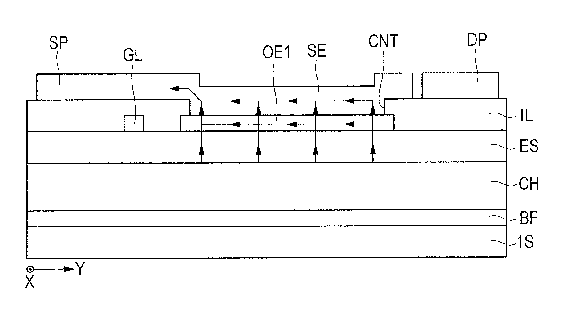
[0132](1) According to the first embodiment, in a process of manufacturing the power MOSFET made of the nitride semiconductor material, the silicon semiconductor process can be applied. This means that the use of the metal film used in the compound semiconductor process can be reduced, as a result of which the manufacturing costs of the power MOSFET in the first embodiment can be reduced.

[0133](2) In this case, the ohmic electrode OE1 (OE2) formed between the power MOSFET made of the nitride semiconductor material, and the interconnect layers (source electrodes SE and drain electrodes DE) is formed of the aluminum film instead of a film including the metal film.

[0134]As a result, in the power MOSFET dealing with a large current, there is a concern about the occurrence of voids and the disconnection caused by the electromigration in th...

first modification

(First Modification)

[0142]In the first embodiment, an example in which the unit electrodes UE1 (UE2) divided from each other are each formed of a single layer film made of the aluminum film is described. In a first modification, an example in which the unit electrodes UE1 (UE2) divided from each other are each formed of a laminated film having the titanium film and the aluminum film will be described.

[0143]FIG. 27 is a diagram illustrating a cross-section of a power MOSFET according to the first modification. The configuration of FIG. 27 is substantially identical with that of FIG. 7 illustrating the first embodiment, and therefore a different feature will be described.

[0144]The feature of the first modification resides in that as illustrated in FIG. 27, each of the plurality of unit electrodes UE1 configuring the ohmic electrode OE1 is formed of a laminated film including a titanium film TI1, an aluminum film AL, and a titanium film TI2. With this configuration, according to the fi...

second modification

(Second Modification)

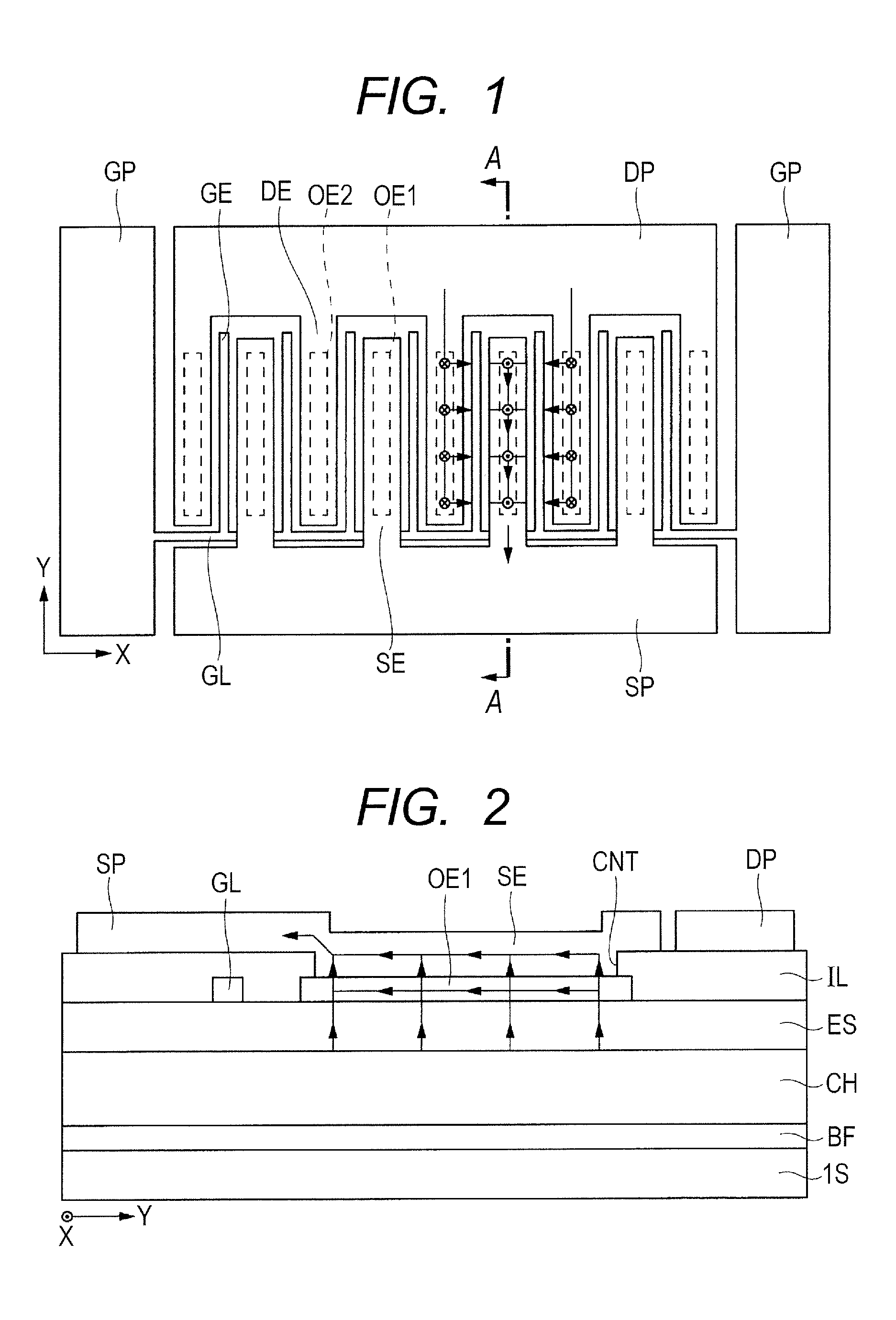
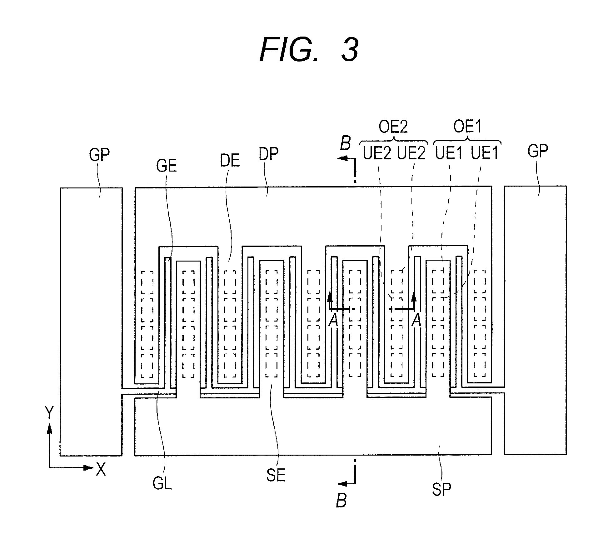
[0148]In the first embodiment, for example, as illustrated in FIG. 3, a case in which the width of the source electrodes SE in the X-axial direction is equal to the width of the drain electrodes DE in the X-axial direction is described. In a second modification, an example in which the width of the source electrodes SE in the X-axial direction is equal to the width of the drain electrodes DE in the X-axial direction will be described.

[0149]FIG. 28 is a diagram illustrating a plan configuration of the power MOSFET according to the second modification. The configuration of FIG. 28 is substantially identical with that of FIG. 3 illustrating the first embodiment, and therefore a different feature will be described.

[0150]A feature of the second modification resides in that the number of unit electrodes UE1 disposed over the lower layer of the source electrodes SE is different from the number of unit electrodes UE2 disposed over the lower layer of the drain electrodes...


PUM


Abstract

The reliability of a field effect transistor made of a nitride semiconductor material is improved. An ohmic electrode includes a plurality of unit electrodes isolated to be separated from each other. With this configuration, an on-state current can be prevented from flowing in the unit electrodes in a y-axial direction (negative direction). Further, in the respective unit electrodes, a current density of the on-state current flowing in the y-axial direction (negative direction) can be prevented from increasing. As a result, an electromigration resistance of the ohmic electrode can be improved.

Description

CROSS-REFERENCE TO RELATED APPLICATIONS[0001]The disclosure of Japanese Patent Application No. 2012-156891 filed on Jul. 12, 2012 including the specification, drawings and abstract is incorporated herein by reference in its entirety.BACKGROUND[0002]The present invention relates to a semiconductor device, and, for example, to a technique that is effectively applied to a semiconductor device including a power device made of a nitride semiconductor material.[0003]Japanese Unexamined Patent Application Publication No. Hei7 (1995)-45829 discloses a configuration in which a plurality of contact holes is connected to a metal wiring portion in a drain diffusion region, and the plurality of contact holes is also connected to a metal wiring portion in a source diffusion region.[0004]Also, Japanese Patent No. 3086713 discloses a technique in which a plurality of source contact regions that joins a source electrode to a nondivided source region is provided.SUMMARY[0005]Nowadays, higher-efficien...

Claims


Application Information

Patent Timeline
Patent Type & Authority Applications(United States)
IPC IPC(8): H01L29/78
CPCH01L29/78H01L29/41H01L29/41725H01L29/517H01L29/518H01L29/66462H01L29/7787H01L29/2003H01L2924/0002H01L2924/00H01L29/205H01L29/452
Inventor OKAMOTO, YASUHIROINOUE, TAKASHINAKAYAMA, TATSUONEGA, RYOHEIKANAZAWA, MASAAKIMIYAMOTO, HIRONOBU
Owner RENESAS ELECTRONICS CORP
Why Eureka
Try Eureka