Method for producing optical electrical field enhancing device

a technology of optical electrical field and enhancement device, which is applied in the direction of optical radiation measurement, instruments, spectrometry/spectrophotometry/monochromators, etc., can solve the problems of difficult formation of fine protrusions and recesses on complex substrates such as liquid containers constituted by a plurality of protrusions and recesses, and reduce manufacturing costs. , the effect of effectively inducing localized plasmons

Inactive Publication Date: 2014-02-06
FUJIFILM CORP
View PDF6 Cites 2 Cited by
  • Summary
  • Abstract
  • Description
  • Claims
  • Application Information

AI Technical Summary

Benefits of technology

[0024]Because an optical electrical field enhancing device can be obtained by these extremely simple steps, manufacturing costs can be greatly reduced compared to those of conventional devices.
[0025]In addition, each of the steps can be applied to substrates having comparatively large areas and substrates having arbitrary shapes. Therefore, it is possible to produce optical electrical field enhancing devices having large areas and optical electrical field enhancing devices having desired shapes.
[0026]An optical electrical field enhancing device obtained by the production method of the present invention is capable of effectively inducing localized plasmon at the surface of the metal structure of fine protru

Problems solved by technology

Therefore, it is considered that the cost of substrates per unit area is high.
In addition, it is extremely difficult to form the aforementioned meta

Method used


Image

  • Method for producing optical electrical field enhancing device
  • Method for producing optical electrical field enhancing device
  • Method for producing optical electrical field enhancing device

Examples


examples

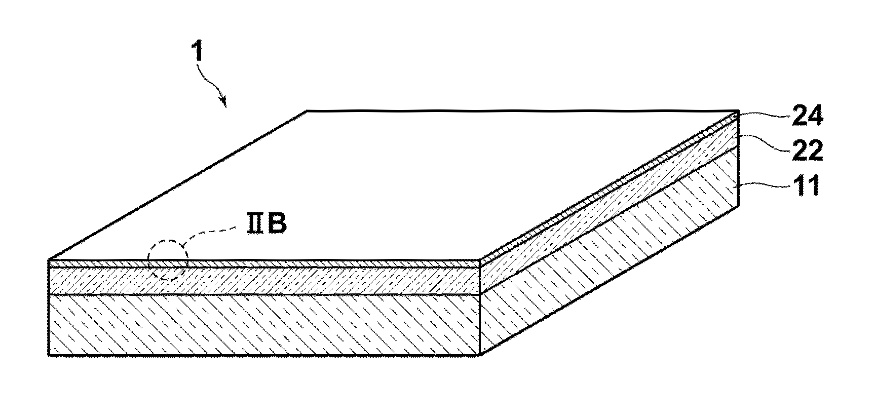
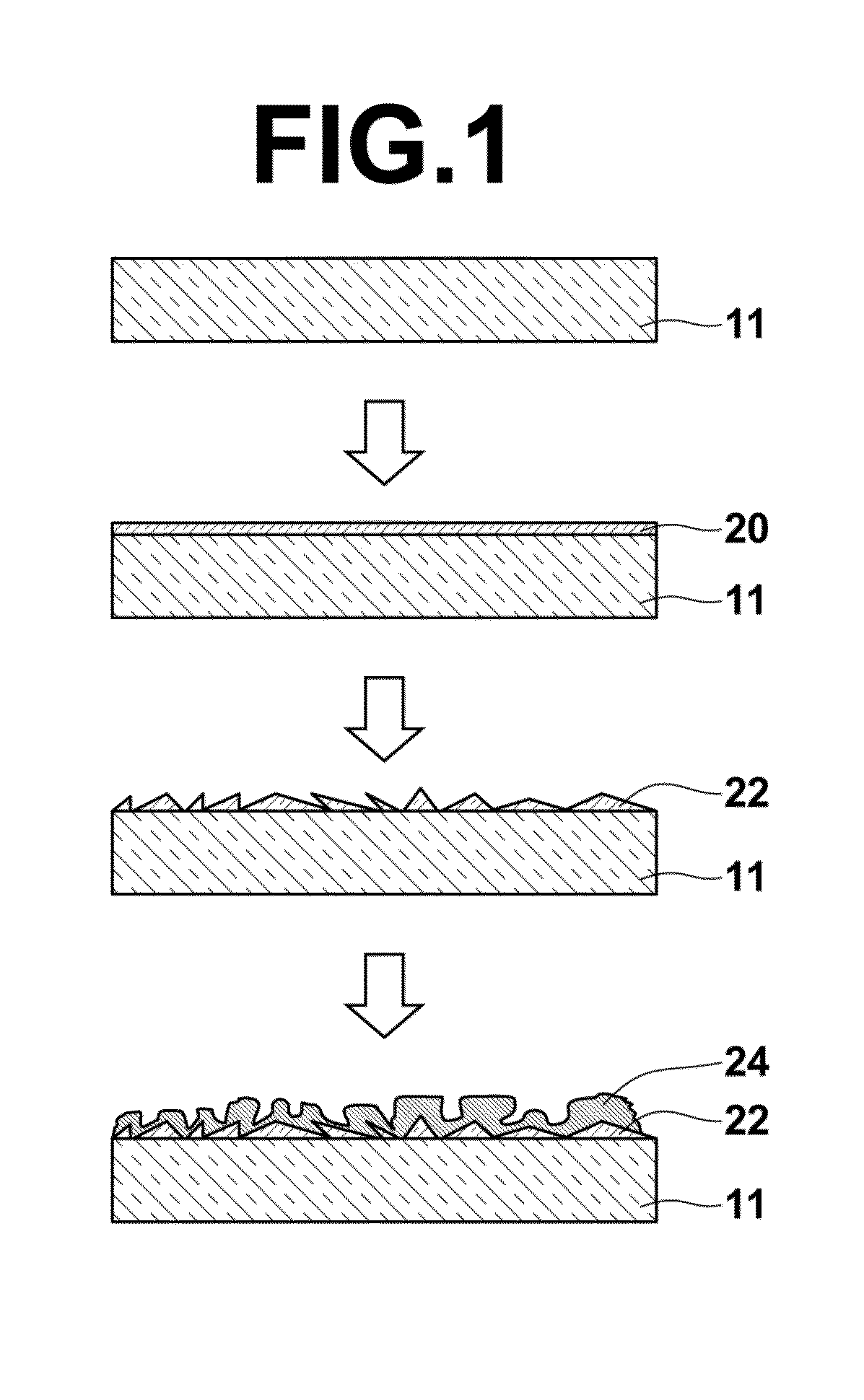
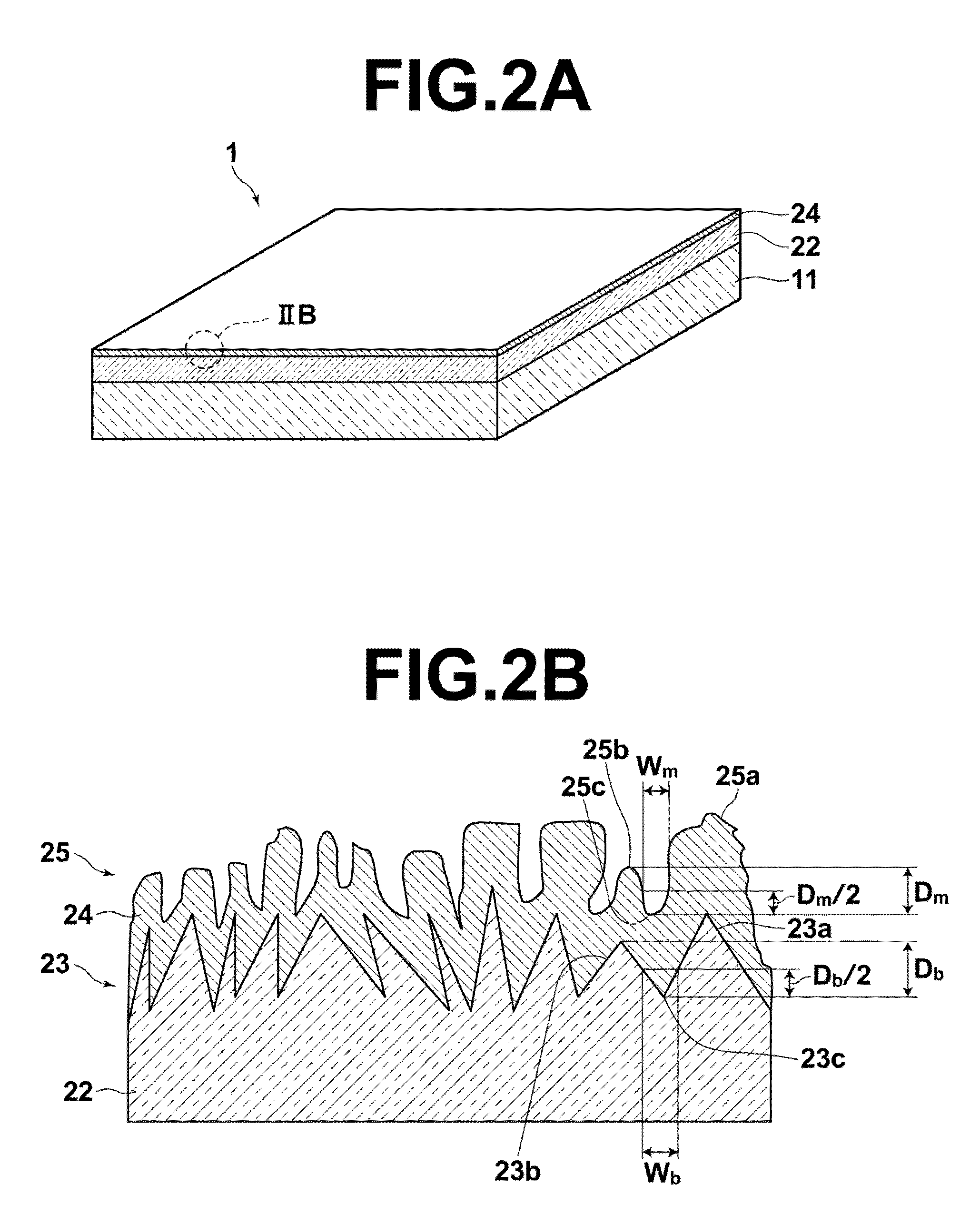
[0081]Hereinafter, concrete production examples of the optical electrical field enhancing substrate 1, which is an embodiment of the optical electrical field enhancing device of the present invention, and the results of Raman spectrum measurement employing measurement samples, will be described.

[Method for Producing Optical Electrical Field Enhancing Substrate]

[0082]A glass substrate (BK-7: Eagle 2000 by Corning) was employed as the transparent substrate main body 11.

[0083]The glass substrate main body 11 underwent ultrasonic cleansing (45 kHz) with acetone for 5 minutes and with methanol for 5 minutes. Then, a 25 nm thick layer of aluminum 20 was formed on the glass substrate 11 using a sputtering apparatus (by Canon Anelva). Note that a surface shape measuring device (by TENCOR) was employed to measure the thickness of the aluminum layer, and the thickness was confirmed to be 25 nm (±100).

[0084]Thereafter, pure water was prepared in a water bath (by Nishi Seiki K. K.) and boiled. ...


PUM

PropertyMeasurementUnit
Thicknessaaaaaaaaaa
Thicknessaaaaaaaaaa
Diameteraaaaaaaaaa

Abstract

A thin film of a first metal or a metal oxide is formed on a substrate. A structure layer of fine protrusions and recesses of the first metal or a hydroxide of the metal oxide is formed by causing the thin film formed on the substrate to undergo a hydrothermal reaction. Thereafter, a metal structure layer of fine protrusions and recesses is formed on the surface of the structure layer of fine protrusions and recesses.

Description

TECHNICAL FIELD[0001]The present invention is related to a method for producing an optical electrical field enhancing device equipped with a metal structure of fine protrusions and recesses capable of inducing localized Plasmon.BACKGROUND ART[0002]Sensor devices that utilize the electrical field enhancing effect due to localized plasmon on the surfaces of metals and electrical field enhancing devices of Raman spectroscopic devices are known. Raman spectroscopy is a technique that obtains the spectrum of Raman scattered light (Raman spectrum) by spectrally analyzing scattered light obtained by irradiating a substance with a single wavelength light beam, and is utilized to identify substances.[0003]There is a Raman spectroscopy technique called SERS (Surface Enhanced Raman Scattering) that utilizes an optical electrical field enhanced by localized plasmon resonance in order to amplify weak Raman scattered light (refer to S. Ghadarghadr et al., “Plasmonic array nanoantennas on layered ...

Claims


Application Information

Patent Timeline
IPC IPC(8): G01J3/44
CPCG01J3/44B82Y20/00G01N21/658B82Y40/00C23C28/322C23C28/345C23C14/18C23C14/5853C03C17/09C03C2218/32
Inventor YAMAZOE, SHOGONAYA, MASAYUKI
Owner FUJIFILM CORP
Why Eureka
Try Eureka