

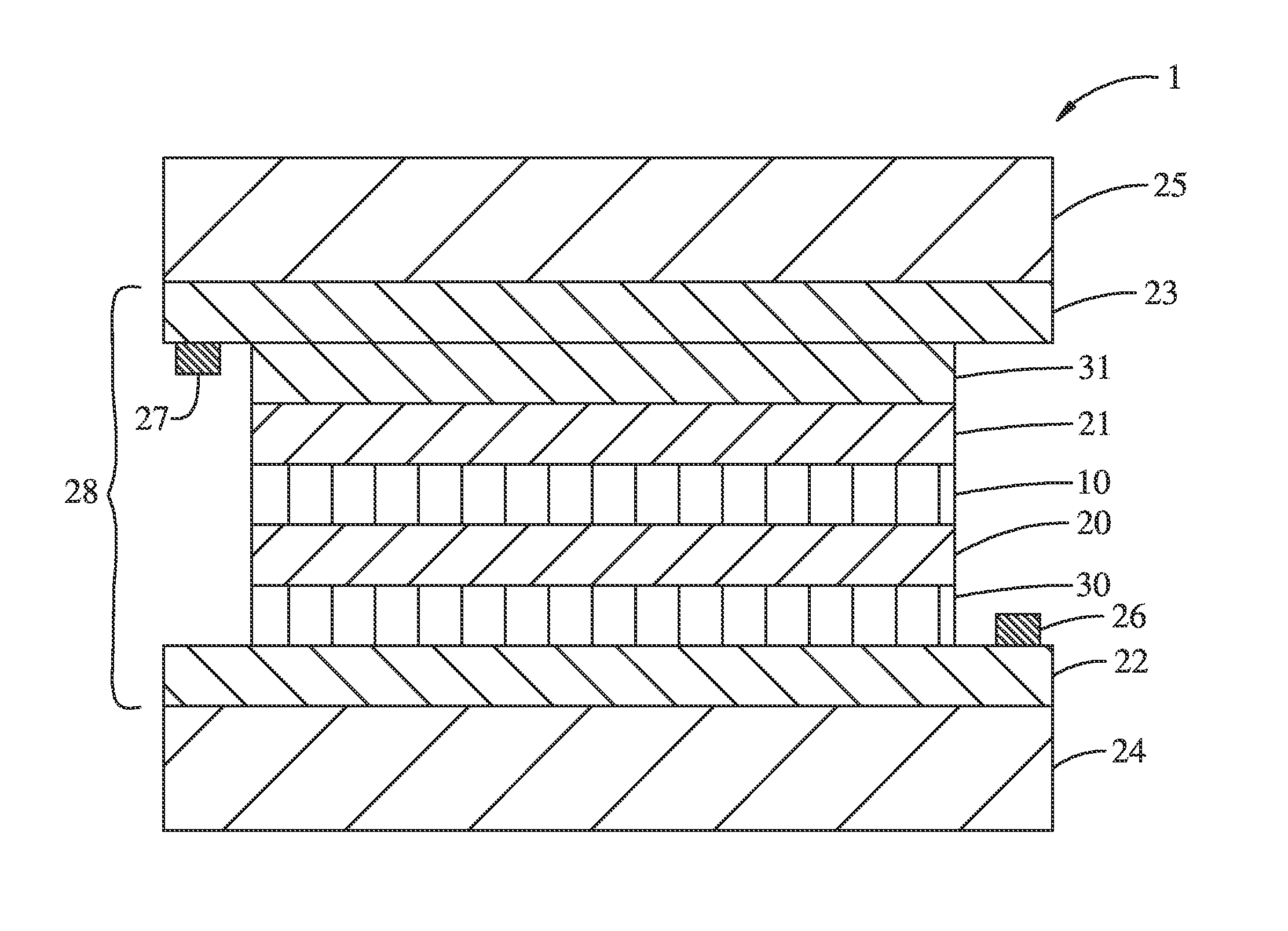
Electrochromic multi-layer devices with current modulating structure
a multi-layer, current modulating technology, applied in the direction of non-linear optics, door/window protective devices, instruments, etc., can solve the problems of non-uniform coloring or switching, non-uniform color or switching, and significant difference between the transmissivity near the edge of the device and the transmissivity at the center of the device, so as to achieve the effect of convenient manufacturing
- Summary
- Abstract
- Description
- Claims
- Application Information
AI Technical Summary
Benefits of technology
Problems solved by technology
Method used
Image

Examples
example 1
Patterned Current Modulating Layer
[0134]A current modulating layer was fabricated on the surface of an electrically conductive layer of Fluorine doped Tin Oxide (FTO) to produce a parabolic cross-layer resistance profile in a direction parallel to one of the sample sides.
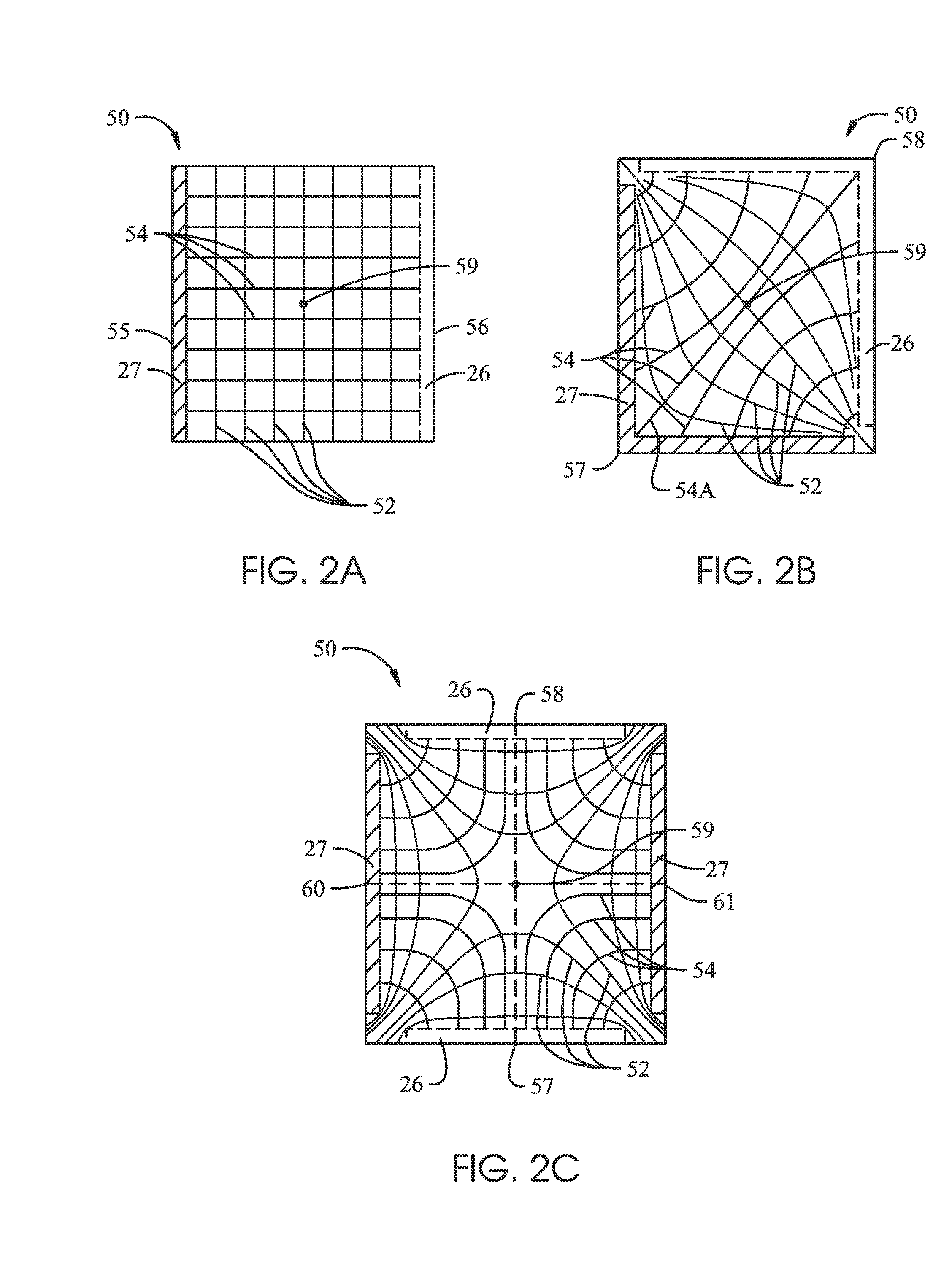
[0135]The substrate material used for this example was 90 mm by 137 mm Pilkington TEC250 (FTO coated soda lime glass) having a sheet resistance of 250Ω / □. The substrate was first cleaned using a 1% solution of Alcanox in water, rinsed with de-ionized water and isopropyl alcohol, then sputter-coated with a 50 nm, uniform film of insulating SiO2. The substrate was then coated with a polymeric positive photoresist, and developed under UV using a photomask purchased from Photo Sciences, Inc. The pattern developed is illustrated schematically on FIG. 4D. The black areas represent areas where the photoresist was developed and removed from the silica coating. The boxes were arranged according to a 1 mm pitch array. The are...
example 2
Patterned Composite Electrically Conductive Layer of Varying Sheet Resistance
[0137]A patterned composite electrically conductive layer was fabricated to produce a linear sheet resistance gradient.
[0138]The substrate material used for this example was 105 mm by 115 mm Pilkington TEC15 (Fluorine doped tin oxide (FTO) coated soda lime glass) having a sheet resistance of 15Ω / □. The substrate was first patterned using a 1064 nm YVO4 laser marking tool, to remove FTO off the surface of the glass in desired areas. The type of pattern used is illustrated schematically in FIG. 20. The areas colored in black represent regions where the TCO has been removed from the surface of the glass. In the present example, the deleted areas are square boxes, arranged in a 1 mm pitch array, where the size of the deleted boxes increase in the direction parallel to the 115 mm side (the direction of the desired gradient), and remain the same in the direction normal to the 115 mm side. The boxes were varied in...
PUM
| Property | Measurement | Unit |
|---|---|---|
| resistivity | aaaaa | aaaaa |
| surface area | aaaaa | aaaaa |
| internal angle | aaaaa | aaaaa |
Abstract
Description
Claims
Application Information