Piezoelectric thin film element

a thin film element and piezoelectric technology, applied in the direction of electrical equipment, metallic material coating process, device material selection, etc., can solve the problems of unfavorable ferroelectric characteristics, unfavorable leakage current characteristics, rapid increase of leakage current, etc., to achieve excellent leakage current characteristics, ferroelectric characteristics, and piezoelectric characteristics.

Active Publication Date: 2014-02-20
MURATA MFG CO LTD
View PDF13 Cites 16 Cited by
  • Summary
  • Abstract
  • Description
  • Claims
  • Application Information

AI Technical Summary

Benefits of technology

[0023]According to the present invention, a piezoelectric thin film element is achieved which has excellent leakage current characteristics, ferroelectric characteristics, and piezoelectric characteristics.

Problems solved by technology

However, the conventional potassium sodium niobate thin films have a problem that while the leakage current is adequately low from 10−7 to 10−6 A / cm2 in an applied electric field of 100 kV / cm, the leakage current is rapidly increased when the electric field exceeds 100 kV / cm, and is 10−2 A / cm2 or more in an applied electric field of 200 kV / cm.
For example, the thin film of the composition (K1-xNax)NbO3 (0
Furthermore, although a ferroelectric hysteresis curve is determined, favorable ferroelectric characteristics have not been achieved.

Method used


Image

  • Piezoelectric thin film element
  • Piezoelectric thin film element
  • Piezoelectric thin film element

Examples


first embodiment

Manufacture of Piezoelectric Thin Film Element

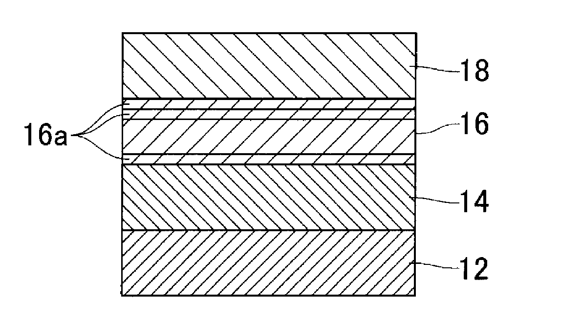
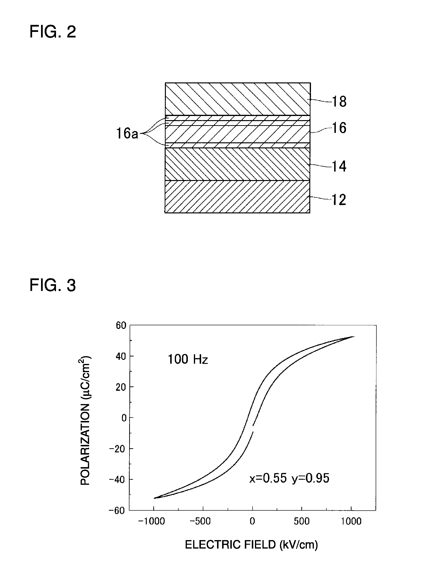
[0035]FIG. 2 is a cross-sectional view schematically illustrating the configuration of a piezoelectric thin film element according to a first embodiment. The piezoelectric thin film element includes a substrate 12, a lower electrode 14 formed on the substrate 12, a piezoelectric thin film 16 formed on the lower electrode 14, and an upper electrode 18 formed on the piezoelectric thin film 16.

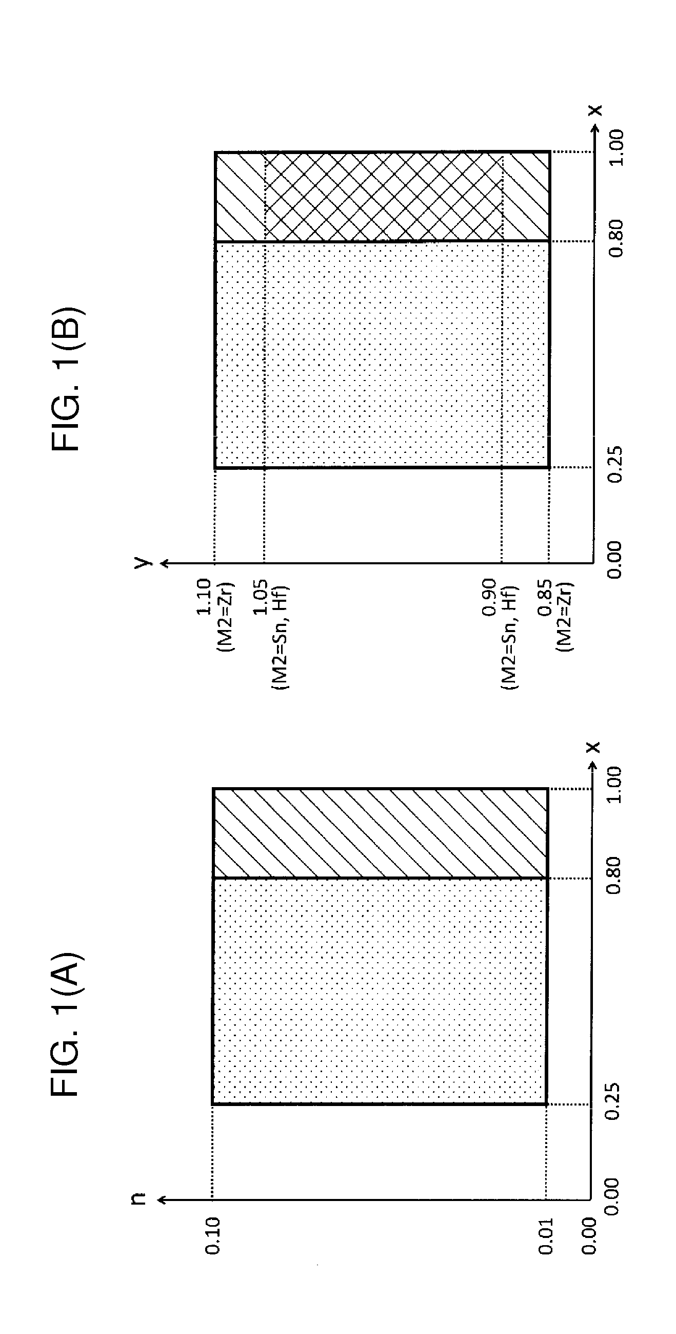
[0036]It is to be noted that the content of BaZrO3 in a potassium sodium niobate thin film represented by the general formula (1−n)(K1-xNax)NbyO3-nBaZrO3 as the piezoelectric thin film 16 is varied in the first embodiment.

[0037]For example, a silicon substrate (Si substrate) is used for the substrate 12. Further, for the substrate 12, substrates may be used such as a glass substrate, a quartz glass substrate, a GaAs substrate, a GaN substrate, a CaF2 substrate, a sapphire substrate, an MgO substrate, an SrTiO3 substrate, an LaAlO3 substrate, a stainle...

second embodiment

Manufacture of Piezoelectric Thin Film Element

[0064]A piezoelectric thin film element according to a second embodiment is configured in the same fashion as the piezoelectric thin film element shown in FIG. 2 according to the first embodiment.

[0065]It is to be noted that the x and y in a potassium sodium niobate thin film represented by the general formula (1−n)(K1-xNax)NbyO3-nBaZrO3 as the piezoelectric thin film 16 are varied in the second embodiment.

[0066]The piezoelectric thin film 16, that is, potassium sodium niobate (KNN) thin film 16 is created by using a chemical solution deposition method.

[0067]First, potassium ethoxide, sodium ethoxide, pentaethoxy niobium, manganese acetylacetonato, barium ethoxide (or calcium ethoxide or strontium ethoxide), and tetraisopropoxy zirconium as raw materials are prepared to meet (1.07−x)×0.97:(x+0.17)×0.97:y×0.97:0.02×0.97:0.03:0.03 in terms of molar ratio. In the case of the present second embodiment herein, x and y respectively satisfy a c...

third embodiment

Manufacture of Piezoelectric Thin Film Element

[0097]A piezoelectric thin film element according to a third embodiment is configured in the same fashion as the piezoelectric thin film element shown in FIG. 2 according to the first embodiment.

[0098]It is to be noted that the content of BaSnO3 in a potassium sodium niobate thin film represented by the general formula (1−n)(K1-xNax)NbyO3-nBaSnO3 as the piezoelectric thin film 16 is varied in the third embodiment.

[0099]The piezoelectric thin film 16, that is, potassium sodium niobate (KNN) thin film 16 is created by using a chemical solution deposition method.

[0100]First, potassium ethoxide, sodium ethoxide, pentaethoxy niobium, manganese acetylacetonato, barium ethoxide, and tetraisopropoxy tin as raw materials are prepared to meet 0.52×(1−n): 0.72×(1−n): 0.95×(1−n): 0.02×(1−n): n:n in terms of molar ratio. In the case of the present third embodiment herein, seven types of 0.00, 0.005, 0.01, 0.03, 0.05, 0.1, and 0.12 are selected as n.

[...


PUM

PropertyMeasurementUnit
thicknessaaaaaaaaaa
grain sizeaaaaaaaaaa
electric fieldaaaaaaaaaa

Abstract

A piezoelectric thin film element that includes a substrate, a lower electrode on the substrate, a piezoelectric film on the lower electrode, and an upper electrode on the piezoelectric film. The piezoelectric film is a potassium sodium niobate film represented, as its main constituent, by the general formula (1−n)(K1-xNax)NbyO3-nM1M2O3 in which M1 is any one of Ca, Sr, and Ba, and M2 is Zr, and x, y, and n respectively are within the ranges of: 0.25≦x≦1.00; 0.85≦y≦1.10; and 0.01≦n≦0.10. Alternatively, M2 is any one of Sn and Hf, and x, y, and n respectively are within the ranges of: 0.25≦x≦1.00; 0.90≦y≦1.05; and 0.01≦n≦0.10.

Description

CROSS REFERENCE TO RELATED APPLICATIONS[0001]The present application is a continuation of International application No. PCT / JP2012 / 059561, filed Apr. 6, 2012, which claims priority to Japanese Patent Application No. 2011-090566, filed Apr. 6, 2011, and Japanese Patent Application No. 2011-264342, filed Dec. 2, 2011, the entire contents of each of which are incorporated herein by reference.FIELD OF THE INVENTION[0002]The present invention relates to a piezoelectric thin film element for use in an actuator, a sensor or the like.BACKGROUND OF THE INVENTION[0003]Piezoelectric bodies are now widely used as materials for functional electronic components such as actuators and sensors. As piezoelectric materials for use in these applications, perovskite-type ferroelectric materials are mainly used which are represented by the general formula Pb(Zr,Ti)O3 referred to as PZT. However, the PZT, which contains harmful Pb (lead), is thus an unfavorable material for protecting the natural environm...

Claims


Application Information

Patent Timeline
Patent Type & Authority Applications(United States)
IPC IPC(8): H01L41/187H01L41/16H01L41/317H01L41/43
CPCH01L41/16H01L41/1873C04B35/495C04B2235/3201C04B2235/3208C04B2235/3213C04B2235/3215C04B2235/3248C04B2235/3251C04B2235/3293C04B2235/6562C04B2235/6567C04B2235/79C23C18/1216C23C18/1225H10N30/1051H10N30/8542H10N30/078H10N30/85H10N30/077
Inventor SHIRAKI, HIROSHI
Owner MURATA MFG CO LTD
Why Eureka
Try Eureka