Programmable logic device

a logic device and programmable technology, applied in the field of programmable logic devices, can solve the problems of increasing power consumption, increasing the number of elements in the entire pld, and increasing the circuit area, so as to achieve the effect of short startup time and less power consumption

Active Publication Date: 2014-04-17
SEMICON ENERGY LAB CO LTD
View PDF18 Cites 21 Cited by
  • Summary
  • Abstract
  • Description
  • Claims
  • Application Information

AI Technical Summary

Benefits of technology

[0011]However, with the structure disclosed in Patent Document 1, regular refresh operation is required to maintain configuration data in the DRAM, and the power consumption is increased as a result. Since the DRAM is a volatile memory, it is necessary to store data in the DRAM every time the PLD is powered on. For this reason, a nonvolatile memory is needed to store configuration data. In addition, a step of transferring a large volume of data from the nonvolatile memory to the DRAM is required every time the PLD is powered on; thus, the startup time is increased.
[0012]When an SRAM is used as the configuration memory, at least four transistors are required, which leads to a significant increase in the number of elements in the entire PLD and an increase in the circuit area.
[0013]In view of the above, an object of one embodiment of the present invention is to provide a PLD that achieves high-speed configuration capable of dynamic configuration, consumes less power, and has a short startup time.

Problems solved by technology

However, with the structure disclosed in Patent Document 1, regular refresh operation is required to maintain configuration data in the DRAM, and the power consumption is increased as a result.
When an SRAM is used as the configuration memory, at least four transistors are required, which leads to a significant increase in the number of elements in the entire PLD and an increase in the circuit area.

Method used


Image

  • Programmable logic device
  • Programmable logic device
  • Programmable logic device

Examples


embodiment 1

[0062]In Embodiment 1, one embodiment of a PLD will be described with reference to FIGS. 1A and 1B, FIG. 2, FIG. 3, and FIG. 4.

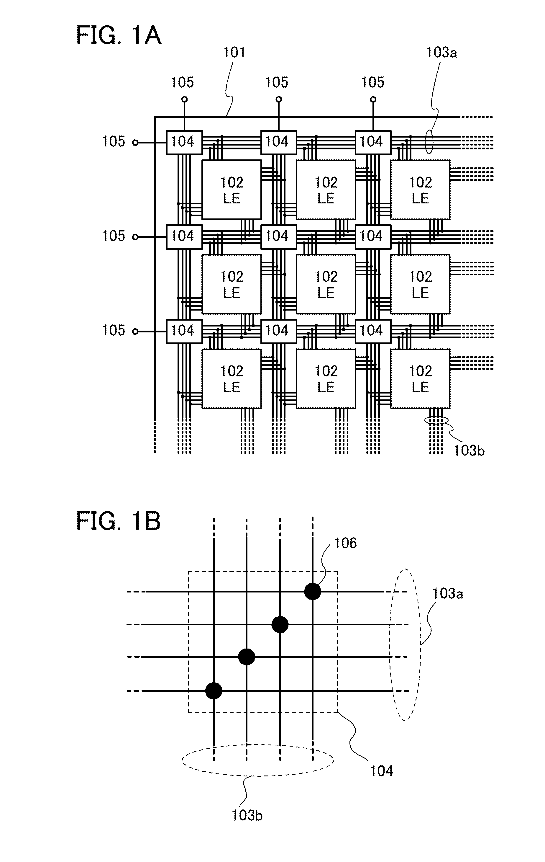
[0063]FIG. 1A conceptually illustrates part of a logic array in the PLD. A logic array 101 includes a plurality of logic elements 102 arranged in an array (the logic element is denoted by LE in FIG. 1A). Here, the term “arranged in an array” means that the logic elements are arranged at regular intervals, and the arrangement is not limited to that illustrated in FIG. 1A.

[0064]A plurality of wirings are formed to surround the logic elements 102. In FIG. 1A, these wirings consist of a plurality of horizontal wiring groups 103a and a plurality of vertical wiring groups 103b. A wiring group is a bundle of wirings, and for example is a bundle of four wirings as illustrated in FIG. 1A. A switch box 104 is provided at an intersection of the horizontal wiring group 103a and the vertical wiring group 103b. The horizontal wiring groups 103a and the vertical wiring gro...

embodiment 2

[0119]In Embodiment 2, a switch 300 in which the n-channel second transistors used in the switch 200 shown in Embodiment 1 are replaced with p-channel second transistors will be described with reference to FIG. 5 and FIG. 6.

(Structure of Switch 300)

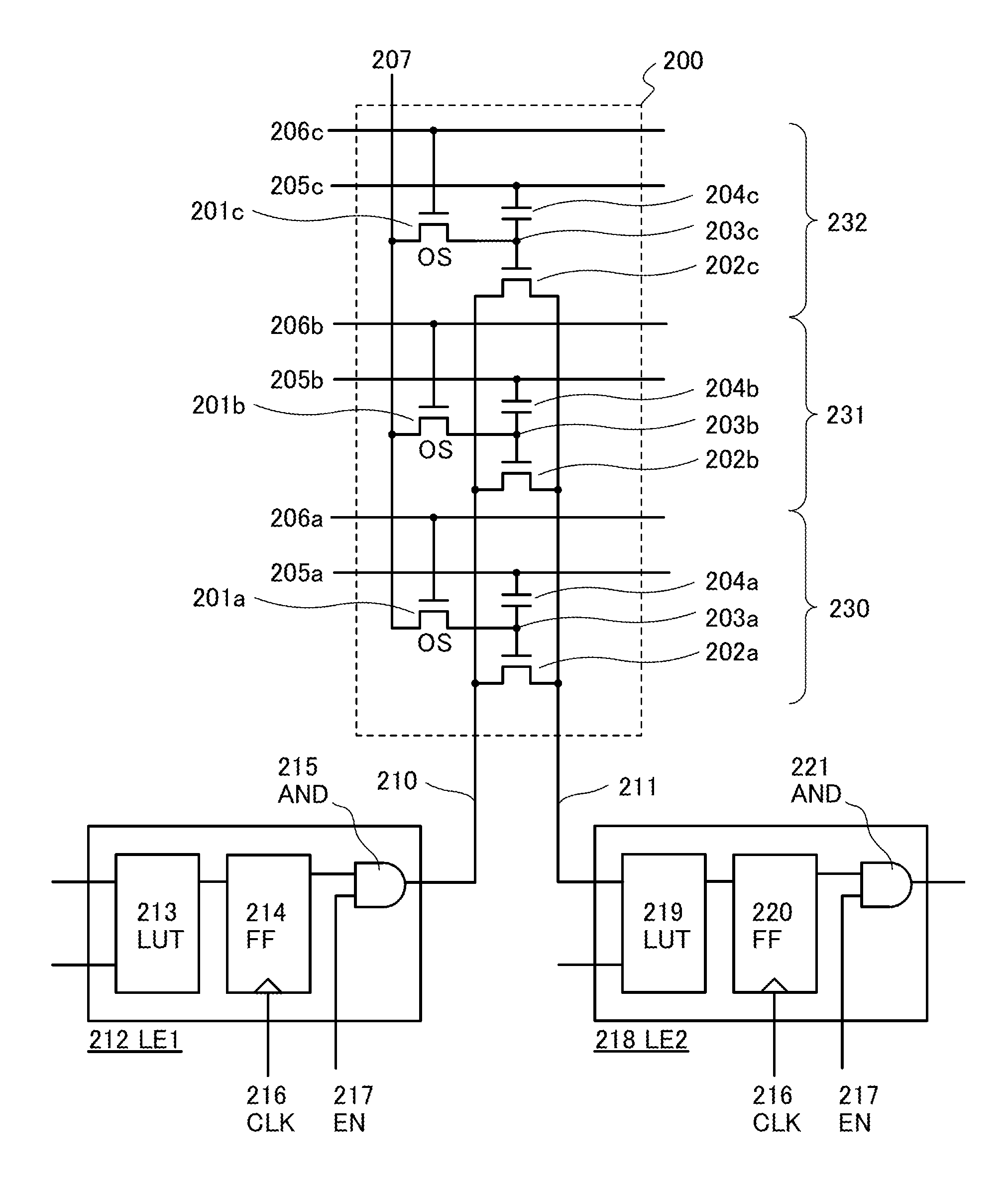
[0120]FIG. 5 illustrates the switch 300 of this embodiment. The structure of the switch 300 is the same as that of the switch 200 in Embodiment 1 except that the n-channel second transistors 202a to 202c are replaced with transistors with opposite polarity, that is, p-channel second transistors 302a to 302c.

[0121]The switch 300 controls connection between a logic element 312 and a logic element 318 in a PLD. For example, in FIG. 5, the logic element 312 can be composed of a lookup table 313, a flip-flop 314, and an AND circuit 315, and the logic element 318 can be composed of a lookup table 319, a flip-flop 320, and an AND circuit 321.

[0122]Like the switch 200 described in Embodiment 1, the switch 300 is composed of a circuit having thre...

embodiment 3

[0151]Embodiment 1 shows the switch 200 using three groups each including a first transistor, a second transistor, and a capacitor, whereas Embodiment 3 will explain a switch 400 including at least three groups (hereinafter referred to as N groups, where N is an integer of 3 or more) of these elements with reference to FIG. 7.

[0152]The switch 400 controls connection between a logic element 412 and a logic element 418 in a PLD. For example, in FIG. 7, the logic element 412 can be composed of a lookup table 413, a flip-flop 414, and an AND circuit 415, and the logic element 418 can be composed of a lookup table 419, a flip-flop 420, and an AND circuit 421.

[0153]As in the switch 200 described in Embodiment 1, the first transistor in the switch 400 uses a semiconductor material that has a wider bandgap and lower intrinsic carrier density than silicon. An oxide semiconductor is used for a channel formation region of the first transistor. Meanwhile, the second transistor is preferably a t...


PUM


Abstract

To obtain a PLD that achieves high-speed configuration capable of dynamic configuration, consumes less power, and has a short startup time and a PLD that has a smaller number of transistors or a smaller circuit area than a PLD using an SRAM as a configuration memory, a plurality of logic elements arranged in an array and a switch for selecting electrical connection between the logic elements are provided. The switch includes a first transistor including a multilayer film including an oxide layer and an oxide semiconductor layer, a node that becomes floating when the first transistor is turned off, and a second transistor in which electrical continuity between a source and a drain is determined based on configuration data held at the node.

Description

TECHNICAL FIELD[0001]The present invention relates to a semiconductor device and particularly to a programmable logic device and a semiconductor device including the programmable logic device. The present invention also relates to an electronic device including the semiconductor device.BACKGROUND ART[0002]Unlike a normal integrated circuit in which all circuits are fixed at the time of manufacture, a programmable logic device (PLD) can function with an intended circuit structure set by a user at the time of actual use after shipment. Examples of such devices that are programmable by users are small ones such as a programmable array logic (PAL) and a generic array logic (GAL) and large ones such as a complex programmable logic device (CPLD) and a field programmable gate array (FPGA); in this specification, such devices are collectively called a programmable logic device (hereinafter referred to as PLD).[0003]PLDs have advantages such as a short development period and flexibility in c...

Claims


Application Information

Patent Timeline
Patent Type & Authority Applications(United States)
IPC IPC(8): H03K19/00
CPCH03K19/0013H03K19/17736H03K19/1776
Inventor YAMAZAKI, SHUNPEIKUROKAWA, YOSHIYUKI
Owner SEMICON ENERGY LAB CO LTD
Why Eureka
Try Eureka