Liquid crystal display device and touch panel

a technology touch panel, which is applied in semiconductor devices, instruments, computing, etc., can solve the problems of varying the power consumption of liquid crystal display device, and achieve the effect of high reliability

Inactive Publication Date: 2014-04-17
SEMICON ENERGY LAB CO LTD
View PDF8 Cites 38 Cited by
  • Summary
  • Abstract
  • Description
  • Claims
  • Application Information

AI Technical Summary

Benefits of technology

[0026]According to the technique disclosed in this specification, a liquid crystal display device having as high reliability a...

Problems solved by technology

It is known that power consumption of liquid crystal display devices varies depend...

Method used


Image

  • Liquid crystal display device and touch panel
  • Liquid crystal display device and touch panel
  • Liquid crystal display device and touch panel

Examples


embodiment 1

Structure of Liquid Crystal Panel

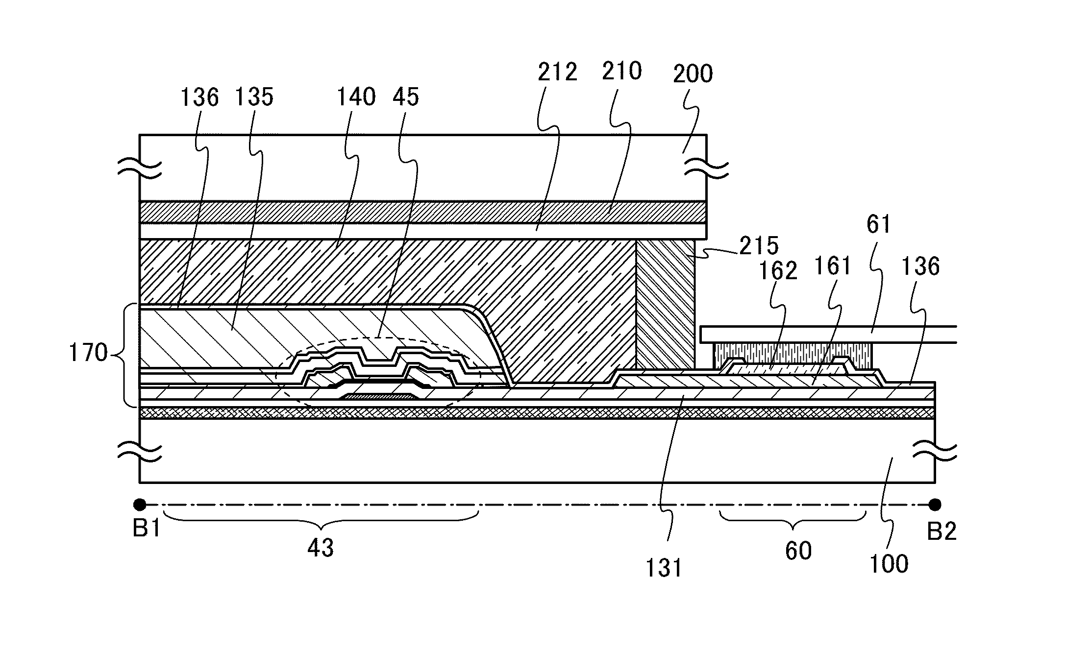
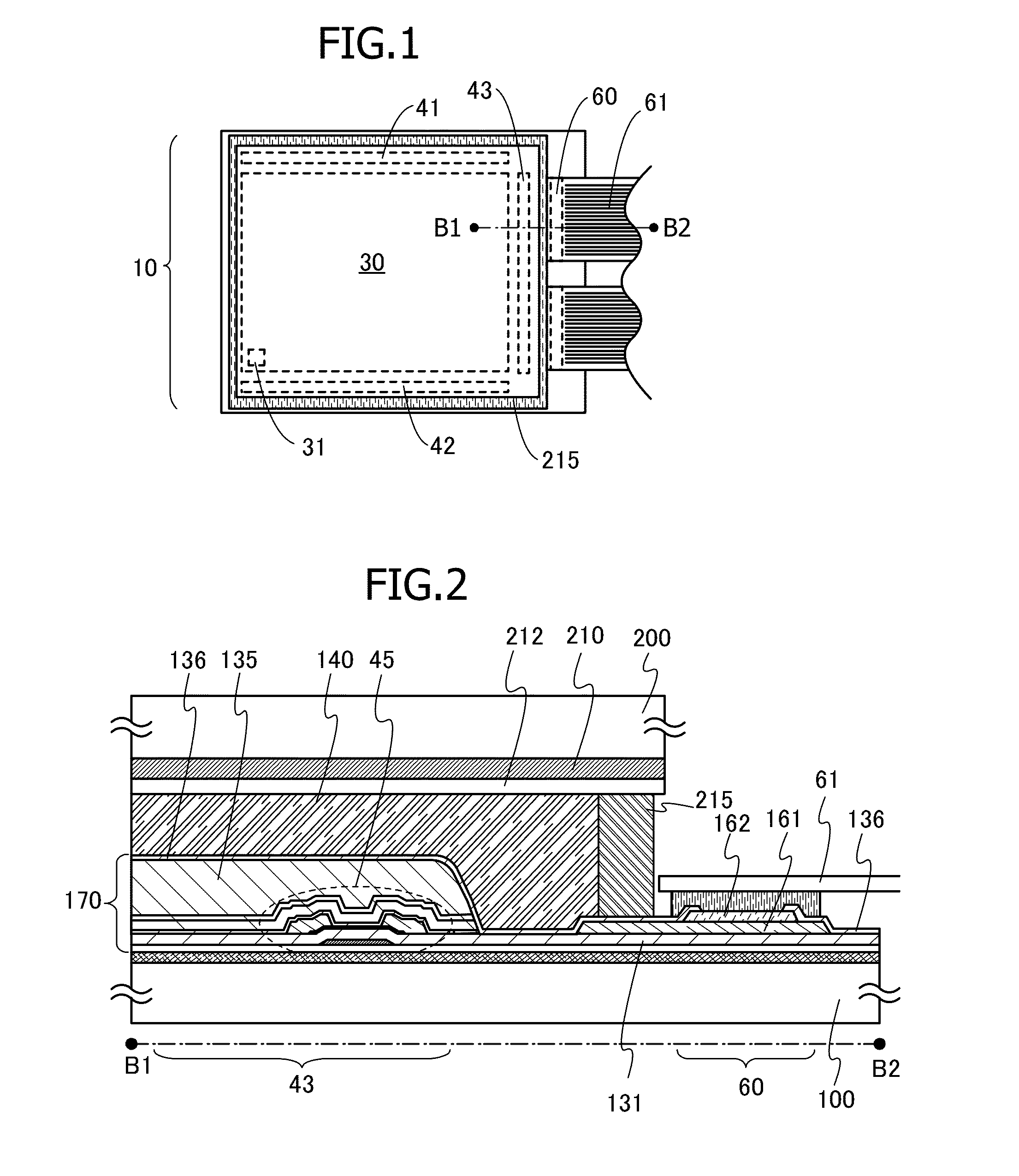
[0062]A liquid crystal panel of this embodiment is described using FIG. 1, FIG. 2, FIG. 3, FIG. 4, FIG. 5, FIG. 14, and FIG. 23. FIG. 1 is a plan view illustrating an example of a structure of a liquid crystal panel 10. FIG. 2 is a cross-sectional view illustrating an example of a structure of the liquid crystal panel 10 and corresponds to a cross-sectional view taken along line B1-B2 in FIG. 1.

[0063]FIG. 23 is a block diagram illustrating an example of a structure of the liquid crystal panel 10. The liquid crystal panel 10 includes a display portion 30, a scan line driver circuit 41, a scan line driver circuit 42, and a data line driver circuit 43. The display portion 30 includes a plurality of pixels 31 connected to scan lines 110 and data lines 111. FIG. 14 is a circuit diagram illustrating a configuration example of the pixel 31.

[0064]The pixel 31 includes a transistor 35 and a liquid crystal element 36. The transistor 35 is a switching element w...

embodiment 2

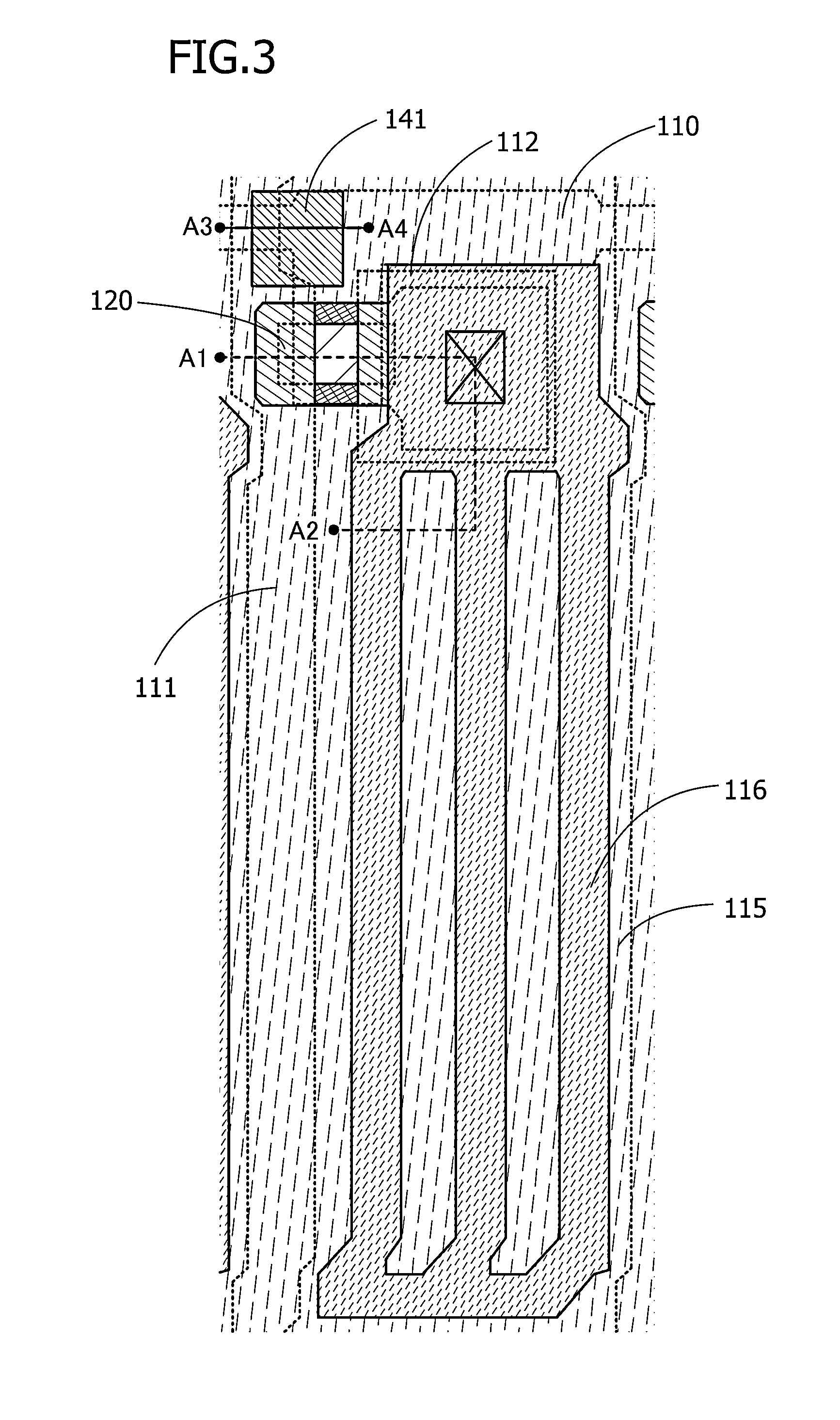
[0170]An oxide semiconductor film forming the semiconductor layer 120 is described in detail.

[0171]The oxide semiconductor film forming the semiconductor layer 120 is classified roughly into a single-crystal oxide semiconductor film and a non-single-crystal oxide semiconductor film. The non-single-crystal oxide semiconductor film includes any of an amorphous oxide semiconductor film, a microcrystalline oxide semiconductor film, a polycrystalline oxide semiconductor film, a c-axis aligned crystalline oxide semiconductor (CAAC-OS) film, and the like.

[0172]The amorphous oxide semiconductor film has disordered atomic arrangement and no crystalline component. A typical example thereof is an oxide semiconductor film in which no crystal part exists even in a microscopic region, and the whole of the film is amorphous.

[0173]The microcrystalline oxide semiconductor film includes a microcrystal (also referred to as nanocrystal) with a size greater than or equal to 1 nm and less than 10 nm, for...

embodiment 3

[0207]The liquid crystal panel 10 in FIG. 1 provided with a touch sensor (contact detector) can function as a touch panel.

[0208]In this embodiment, a touch panel is described with reference to FIG. 10, FIG. 11, and FIGS. 12A and 12B.

[0209]FIG. 10 is a cross-sectional view illustrating a structure example of a touch panel 400 using the liquid crystal panel 10. The touch panel 400 includes a capacitive sensor as a touch sensor. A polarizing plate 411 is attached to the outer side of the substrate 100, and a polarizing plate 412 is attached to the inner side of the substrate 200. Note that the polarizing plate 412 may be provided on the outer side of the substrate 200.

[0210]A common electrode 421 over the substrate 100 serves as a common electrode of a pixel and an electrode of a capacitor in the touch sensor. An electrode 422 is provided on the outer side of the substrate 200. In the case where the polarizing plate 412 is provided on the outer side of the substrate 200, the electrode ...


PUM


Abstract

To provide a highly reliable liquid crystal display device including flexible substrates and a crystalline oxide semiconductor film for a backplane. The device includes a flexible first substrate, a flexible second substrate facing the first substrate, and a liquid crystal layer sealed between the substrates with a sealing member. The first substrate is provided with a layer including a transistor, an organic resin film over the transistor, a pixel electrode and a common electrode over the organic resin film, which partly overlap with each other with an insulating film provided therebetween, and an alignment film thereover. The transistor includes a crystalline oxide semiconductor film as a semiconductor layer where a channel is formed. Drying treatment is performed on the layer before the liquid crystal layer is sealed between the substrates, and steps from the drying treatment to sealing of the liquid crystal layer are performed without exposure to the air.

Description

BACKGROUND OF THE INVENTION[0001]1. Field of the Invention[0002]The present invention relates to a liquid crystal display device including a transistor using an oxide semiconductor film and a touch panel including the liquid crystal display device.[0003]2. Description of the Related Art[0004]Transistors which are used for many liquid crystal display devices and organic EL display devices have been formed using a silicon semiconductor film such as an amorphous silicon film or a polycrystalline silicon film.[0005]Instead of the silicon semiconductor film, a technique in which an oxide semiconductor film is used for transistors has attracted attention.[0006]For example, a technique is disclosed in which a transistor manufactured using an In—Ga—Zn oxide film as an oxide semiconductor film is used as a switching element or the like of a pixel (see Patent Documents 1 and 2).[0007]Further, we develop a technique in which an oxide semiconductor film having a noble crystal structure is manuf...

Claims


Application Information

Patent Timeline
IPC IPC(8): G02F1/1333
CPCG02F1/13338G02F1/133305G06F3/0412G06F2203/04103G06F3/0443G06F3/0445G06F3/0446G02F1/13415H01L27/1225H01L29/7869H01L29/78696G02F1/136G02F1/1333G02F1/133345G02F1/1341G02F1/134309G02F1/1368G02F2201/121G02F2201/123G02F2202/10H01L29/045
Inventor YAMAZAKI, SHUNPEIHIRAKATA, YOSHIHARUKUBOTA, DAISUKEYAMASHITA, AKIO
Owner SEMICON ENERGY LAB CO LTD
Why Eureka
Try Eureka