Trench gate type semiconductor device and method of producing the same

a semiconductor device and clamp gate technology, applied in semiconductor devices, diodes, electrical devices, etc., can solve the problems of difficult protection of side walls, and achieve the effect of preventing excessive electric fields and good ohmic conta

Active Publication Date: 2014-05-22
FUJI ELECTRIC CO LTD
View PDF0 Cites 7 Cited by
  • Summary
  • Abstract
  • Description
  • Claims
  • Application Information

AI Technical Summary

Benefits of technology

[0039]As another measure, there is a method disclosed in JP-A-2007-194283 and corresponding US Patent Appln. 2007187695. When this method is applied to the SiC trench gate type MOSFET shown in FIG. 37, an embedding insulator 15 is embedded in a lower portion of each trench 10 while the trench 10 has a depth to reach a drain-side highly doped layer (a field stopping layer 2 in FIG. 68) as shown in FIG. 68. According to this structure, breakdown is avoided because an electric field substantially equal to that applied to the voltage withstanding layer 3 is applied to the embedding insulator 15 based on the electromagnetic law regardless of the relative dielectric constant if the trench 10 can reach the field stopping layer 2.
[0042]As for the function of protecting the insulating film in the bottom of each trench from an excessive electric field as described in JP-A-8-204179, firstly there is provided a structure in which the maximum electric field at off-time is produced near the Schottky electrode, not the insulating film in the bottom of each trench, to prevent the insulating film from being broken down. Secondly the voltage withstanding layer is pinched off by the depletion region extending from the Schottky electrode adjacent at off-time to thereby prevent an excessive electric flux line from reaching the gate trench.
[0045]Although the use of the second function permits a high withstand voltage to be achieved by a thinner voltage withstanding layer and a higher Schottky barrier compared with the first function, there is a possibility that on-state-resistance will increase because the current flow path at on-state is narrowed by the depletion region extending from the Schottky contact, for example, in the same manner as in the case where an embedded region of a conductivity type reserve to the voltage withstanding layer is provided in the bottom of the gate trench as shown in FIG. 67. However, increase in on-state-resistance can be suppressed because the built-in potential of the Schottky contact is lower than that of a pn junction so that the extension of the depletion region at on-state in the Schottky contact is smaller than that in the pn junction.
[0046]In view of the above, the invention further provides a trench gate type semiconductor device and a method of producing the same, for example illustrated in Embodiments 8-10, in which an excessive electric field is prevented from being applied to an insulating film in the bottom of each trench while the second object can be satisfied.
[0066]According to the invention, there can be provided a trench gate type semiconductor device and a method of producing the same, in which the cell pitch can be made smaller than that in the related art even when a semiconductor material not established yet as a mass-production method for impurity doping due to a thermal diffusion method is used. Moreover, there can be provided a trench gate type semiconductor device and a method of producing the same, in which good ohmic contact can be obtained without use of selective epitaxial growth for at least one conductivity type while the first object can be satisfied. In addition, there can be provided a trench gate type semiconductor device and a method of producing the same, in which an excessive electric field is prevented from being applied to an insulating film in the bottom of each trench while the second object can be satisfied.

Problems solved by technology

It is however difficult to protect the side wall because the width of the trench 10 is, for example, no more than 0.6 μm.

Method used


Image

  • Trench gate type semiconductor device and method of producing the same
  • Trench gate type semiconductor device and method of producing the same
  • Trench gate type semiconductor device and method of producing the same

Examples


embodiment 1

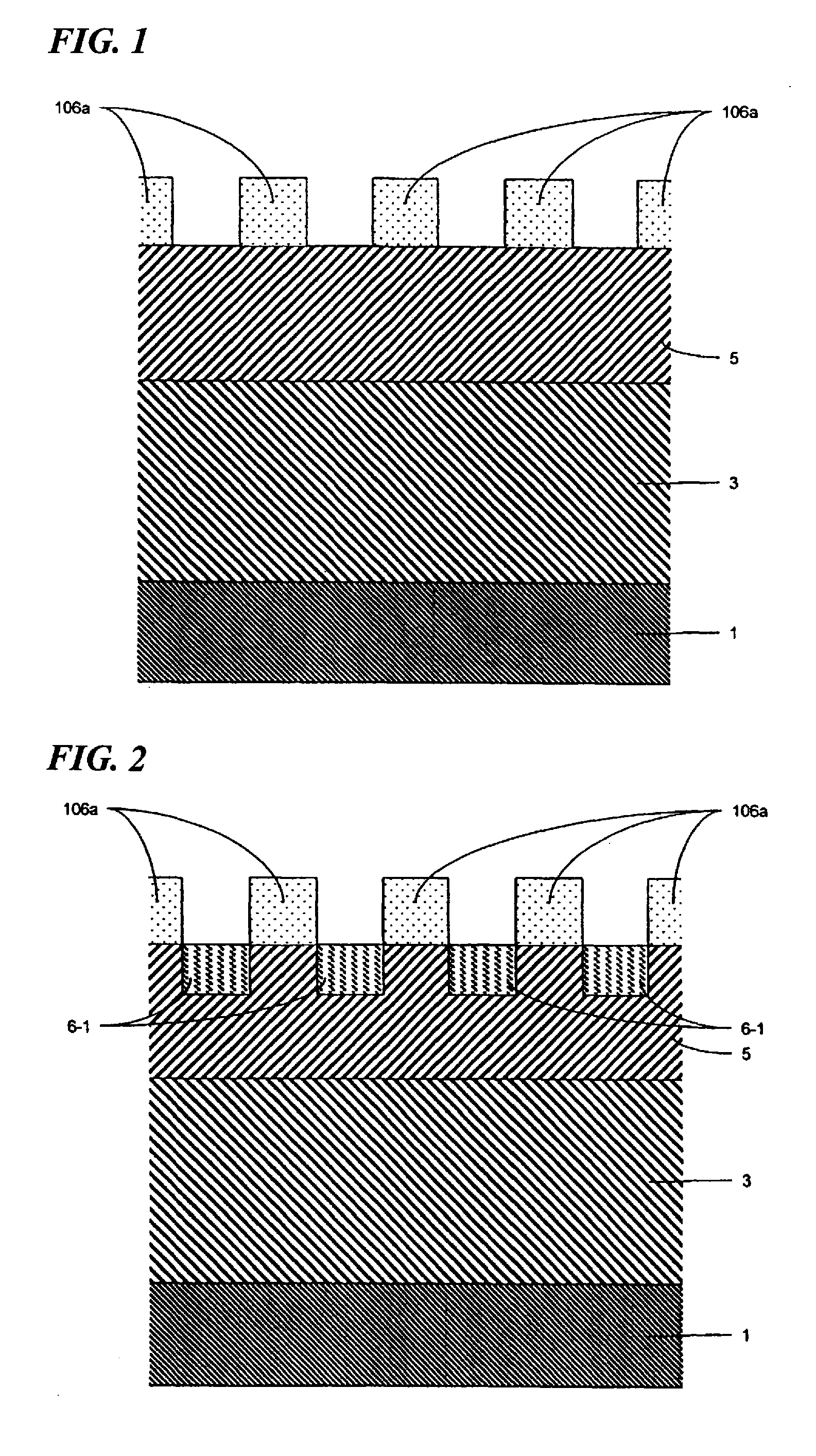
[0139]As shown in FIG. 1, a voltage withstanding layer 3 having a predetermined doping concentration of an n type and a predetermined thickness and a body layer having a predetermined doping concentration of a p type and a predetermined thickness are formed successively by epitaxial growth on the whole area of one principal surface (referred to as front surface) of an n-type SiC substrate 1. A predetermined first mask layer, for example, made of an SiO2 film is formed on a front surface of the body layer. The mask layer is patterned to form a first mask 106a having a predetermined first opening portion by photolithograpy. Although a SiO2 film is preferred as the first mask, another material may be used. In principle, the term “body region” means a region formed selectively on the wafer surface and the term “body layer” means a layer formed fully on the wafer surface. However, strict discrimination between layer and region may not be made in the following description because it may b...

embodiment 2

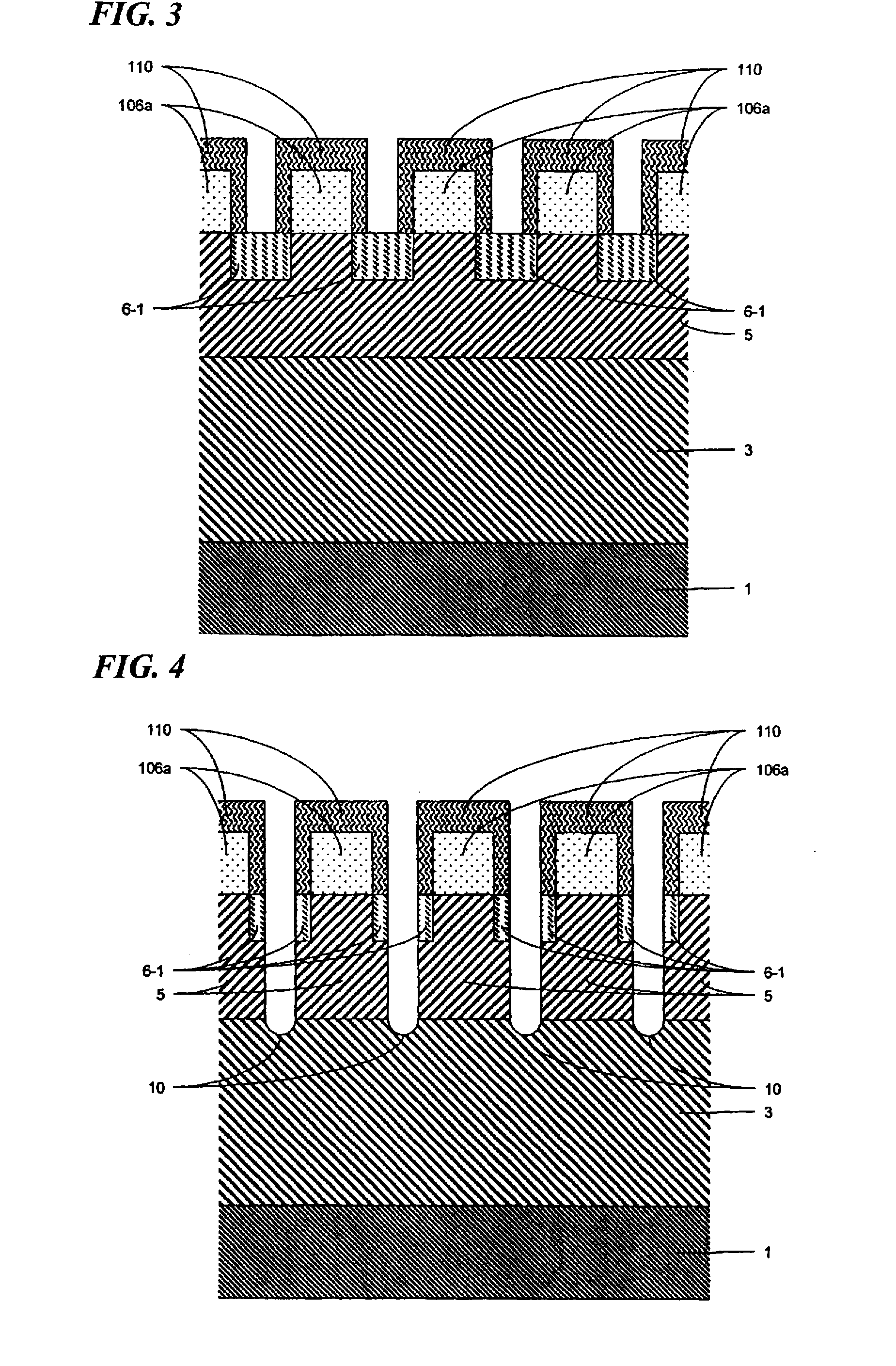
[0144]When nonselective, i.e. full epitaxial growth is an essential or effective method for forming body contact regions 7, a body contact layer 7-1 is first formed on the whole front surface of a body region 5 as shown in FIG. 5. As for the body contact layer 7-1, doping may be performed simultaneously with epitaxial growth to provide a predetermined doping concentration in order to obtain good ohmic contact, or the composition of alloys may be controlled in a growth direction to form a predetermined quantum well structure. Alternatively, the two characteristics may be used in combination. Description will be made topically on the fact that source regions 6, body contact regions 7 and trenches 10 can be formed by self-alignment from the state shown in FIG. 5.

[0145]First, as shown in FIG. 6, a first mask 106a having predetermined first opening portions is formed. Then, anisotropic etching is performed with use of the first mask 106a as a mask to partially remove the body contact lay...

embodiment 3

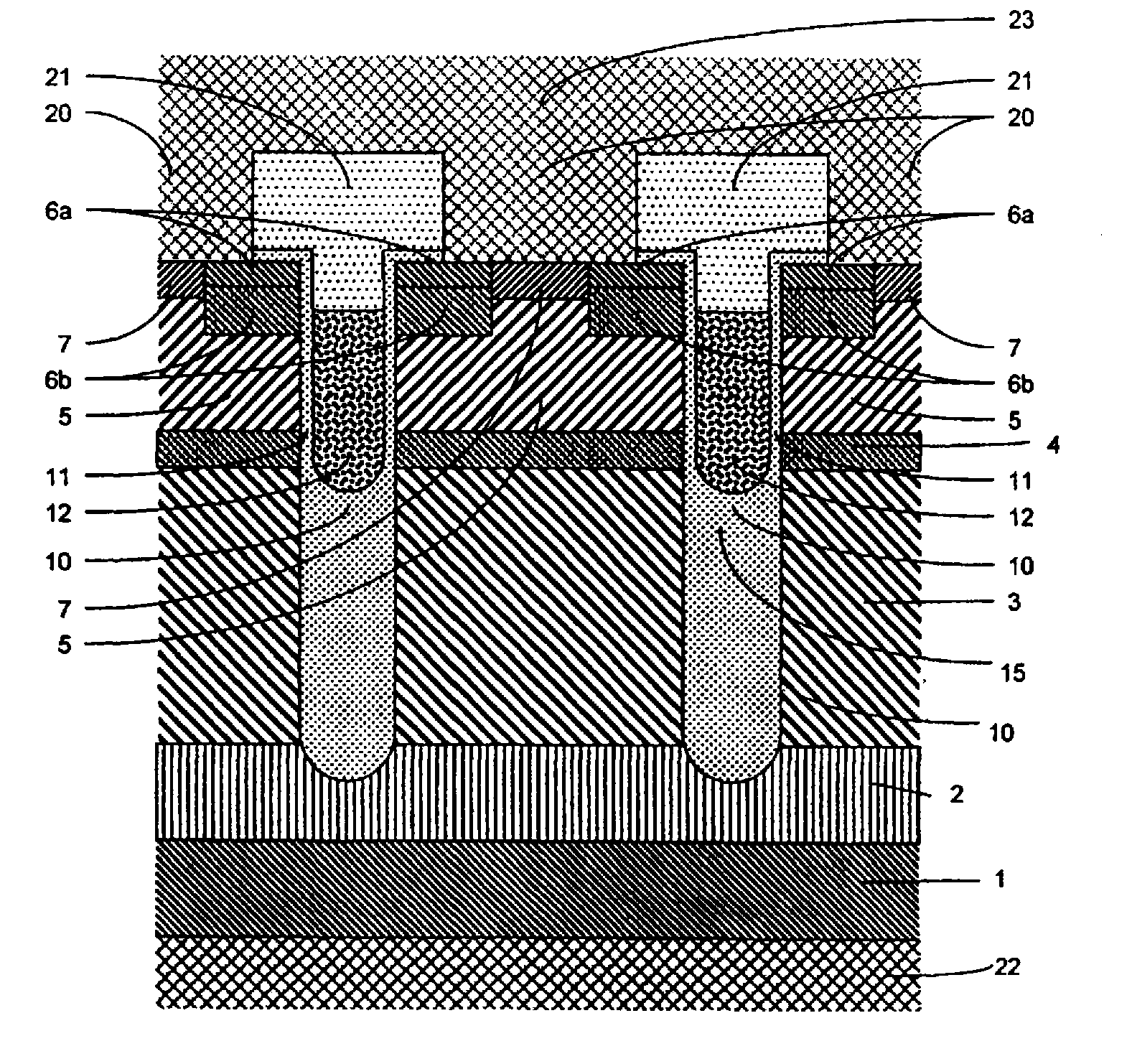
[0148]Because the producing method according to Embodiment 1 and the producing method according to Embodiment 2 make it possible to form each trench 10 narrower than the resolution limit of the used stepper or the like, the production margin at etching back can be enlarged when a gate electrode or the like to be embedded in each trench 10 is formed by etching back. However, when such a semiconductor material that the temperature for impurity doping due to a thermal diffusion method cannot be said to be practical in an ordinary production process is used, there may occur a second problem that the production margin at etching back is still short because the depth of each source region 6 is limited by the ion implantation device. The producing method according to Embodiment 3 is provided as a modification adapted for such a case.

[0149]First, a body contact layer 7-1 is formed on each body region 5 in accordance with necessity. Although this film-forming is not an essential process, des...


PUM


Abstract

A method of producing a trench gate type MOSFET is provided in which each intersection trench is formed as a two-stage trench structure. A gate trench is backfilled with a mask material and the mask material is then patterned to form a mask used for forming each intersection trench. The intersection trench intersecting the gate trench is provided so as to be deeper than the gate trench. A Schottky electrode is provided in the bottom of each intersection trench 10p. In this manner, there is provided a trench gate type semiconductor device and a method of producing the same, in which: the cell pitch can be reduced even when a wide band gap semiconductor is used as a main semiconductor substrate; good ohmic contacts can be obtained; and an excessive electric field is prevented from being applied to an insulating film in the bottom of each trench.

Description

BACKGROUND[0001]The present invention relates to a semiconductor device having a trench gate structure and a method of producing the same. More specifically, the invention relates to a trench gate type semiconductor device using silicon carbide semiconductor (hereinafter abbreviated to SiC) or Group III nitride semiconductor such as AlGaN semiconductor and a method of producing the same.[0002]When a high withstand voltage power device is produced from silicon carbide semiconductor (hereinafter referred to as SiC) or Group III nitride semiconductor (hereinafter referred to as AlGaN or the like), there is a possibility that on-state-resistance will be remarkably reduced. On-state-resistance of 5 mΩcm2 or lower is obtained by a MISFET of a 1-1.2 kV withstand voltage class using SiC. The on-state-resistance is not higher than that of an IGBT made of a silicon semiconductor (hereinafter referred to as Si) of the same withstand voltage class. There is a possibility that the majority of IG...

Claims


Application Information

Patent Timeline
Patent Type & Authority Applications(United States)
IPC IPC(8): H01L29/66H01L21/28H01L21/265H01L21/308
CPCH01L29/0623H01L29/0696H01L29/086H01L29/0878H01L29/1608H01L29/41766H01L29/4236H01L29/42368H01L29/47H01L29/66068H01L29/7806H01L29/7813H01L21/265H01L21/28008H01L21/308H01L29/66666H01L21/02378H01L21/0337H01L29/66522H01L29/66848
Inventor NAKAMURA, SHUN-ICHIKAWADA, YASUYUKI
Owner FUJI ELECTRIC CO LTD
Why Eureka
Try Eureka