Ion implantation apparatus

a technology of implantation apparatus and ion ion, which is applied in the direction of vacuum evaporation coating, chemical vapor deposition coating, coating, etc., can solve the problems of significant increase in power consumption, uneven implantation angle to a wafer, and inability to obtain the characteristics of a semiconductor device as expected, etc., to achieve sufficient work area and simplify setting and preparation

Active Publication Date: 2014-06-05
SUMITOMO HEAVY IND ION TECH
View PDF1 Cites 23 Cited by
  • Summary
  • Abstract
  • Description
  • Claims
  • Application Information

AI Technical Summary

Benefits of technology

[0029]Therefore, in the present embodiment, the high-energy ion implantation apparatus having the following configuration can suppress the installation area while ensuring the workability for the ion implantation apparatus.

Problems solved by technology

If the valence is changed during passage of the magnetic field collimating magnet, a deflection angle of collimation is changed, and thus an implantation angle to a wafer is not uniform.
However, the measured value fluctuates out of an expected implantation value according to the change of the valence, and thus characteristics of a semiconductor device are not obtained as expected.
Therefore, in order to safely install and maintain the apparatus, it is necessary to reinforce a strength design of a semiconductor factory itself, and power consumption significantly increases.
However, in this case, the total length of the apparatus becomes very long, setting and preparation of an installation site, installation work, and the like become complicated, and the installation area is also increased.
Also, adjustment of fixing alignment of each device, maintenance or repair of the apparatus after the operation, and work space for adjustment are also required.
Such a large-scale ion implanter cannot satisfy requirements for adjusting the apparatus size in the semiconductor manufacturing line to the actual circumstances of the production line arrangement of the factory.

Method used


Image

  • Ion implantation apparatus
  • Ion implantation apparatus
  • Ion implantation apparatus

Examples


Embodiment Construction

[0025]The invention will now be described by reference to the preferred embodiments. This does not intend to limit the scope of the present invention, but to exemplify the invention.

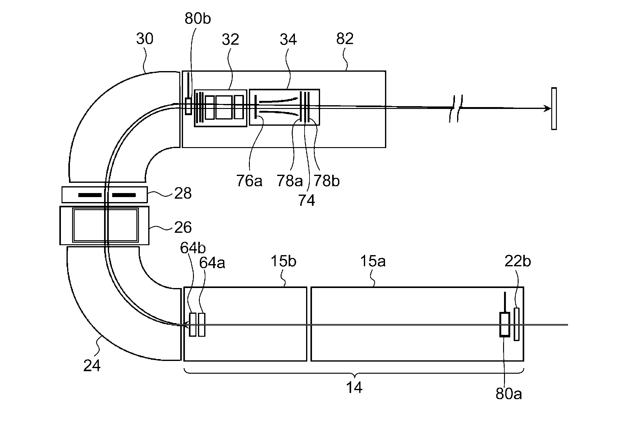
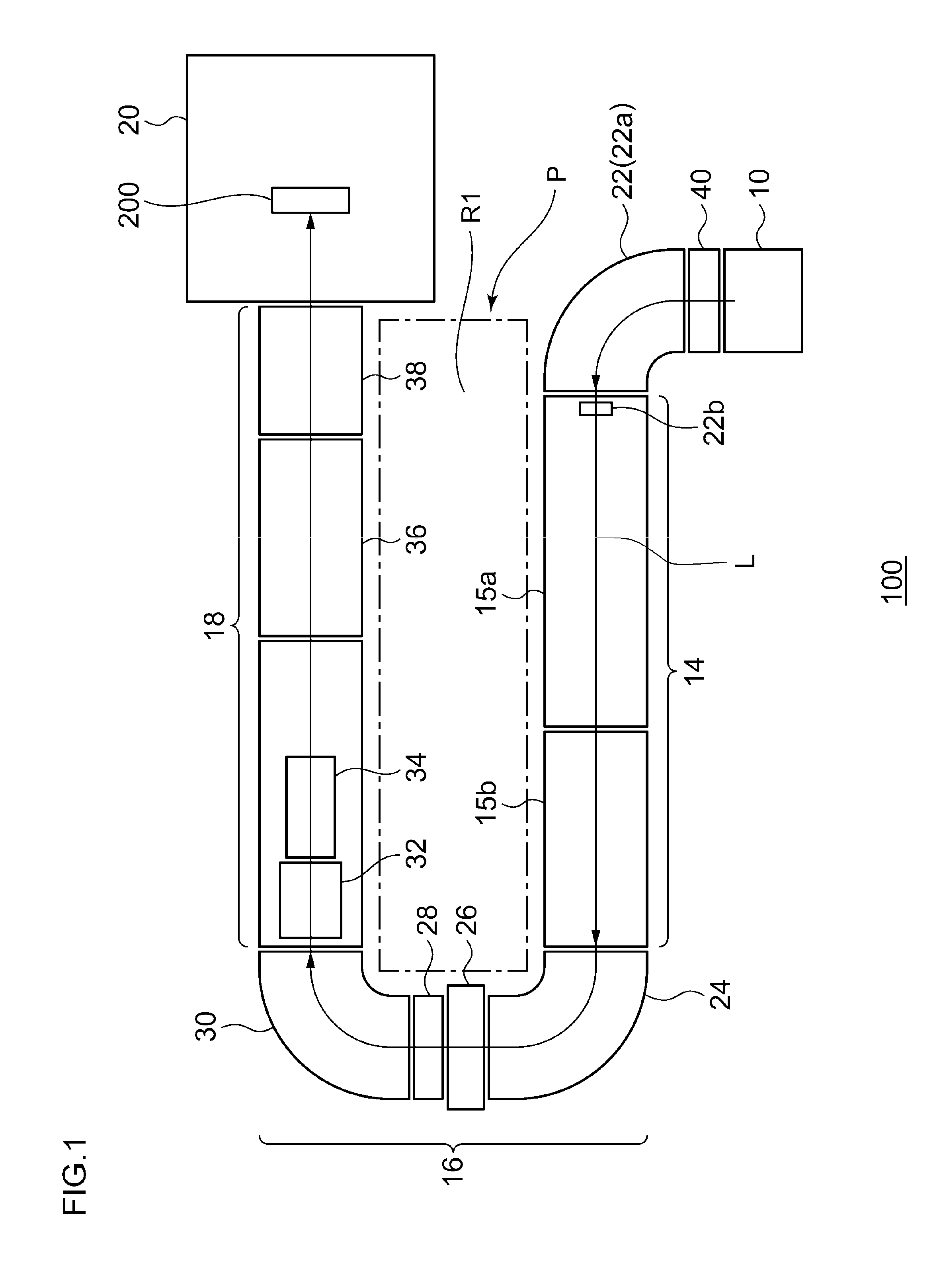
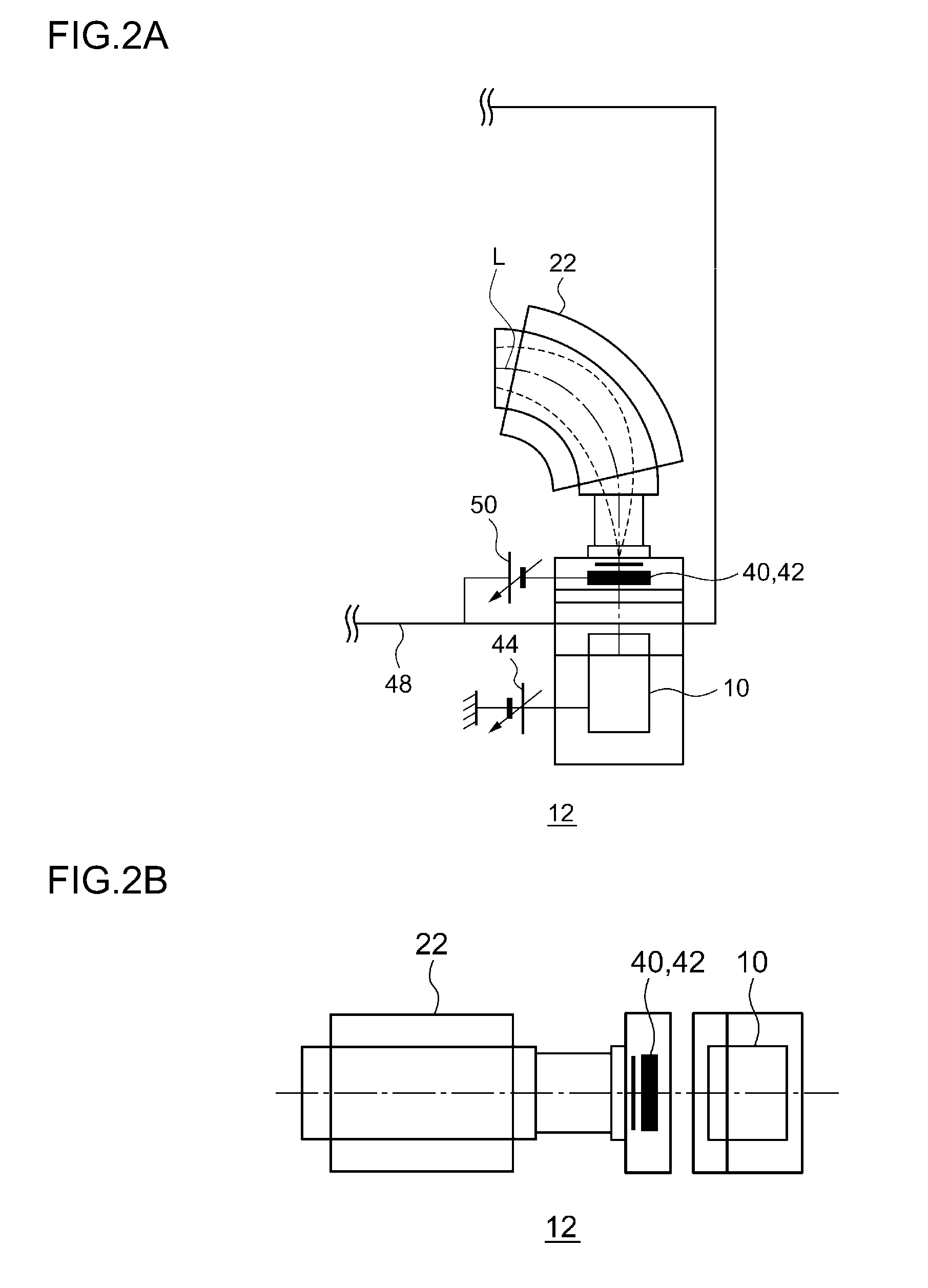
[0026]A high-energy ion implantation apparatus capable of implanting ions having high energy (for example, 1 to 4 MeV) into a substrate includes a plurality of constituent devices, for example, an ion source, a mass analysis magnet, a radio-frequency linear accelerator (linac), a beam transport system including an energy filter, a beam scanner, a beam collimator, a final energy filter, an implantation processing chamber, and a substrate transfer device. Therefore, if each of the constituent devices is independently fixed on a substantially straight line, the total length becomes very long, which requires much effort on fixing alignment of each device, maintenance, adjustment, and repair after operation.

[0027]Also, if each constituent device of the high-energy ion implantation apparatus is independently m...


PUM

PropertyMeasurementUnit
total deflection angleaaaaaaaaaa
deflection angleaaaaaaaaaa
total lengthaaaaaaaaaa

Abstract

An ion implantation apparatus includes: a plurality of units for accelerating an ion beam generated in an ion source; and a plurality of units for adjusting a scan beam and implanting ions into a wafer. A horizontal U-shaped folder type beamline having opposite long straight portions includes the plurality of units for adjusting the scan beam in a long straight portion to have substantially the same length as the ion source and the plurality of units for accelerating the ion beam.

Description

BACKGROUND OF THE INVENTION[0001]1. Field of the Invention[0002]The present invention relates to an ion implantation apparatus.[0003]2. Description of the Related Art[0004]In a semiconductor device manufacturing process, an important process for making the semiconductor wafer into a semiconductor device is performed by adding impurities to a crystal of a semiconductor wafer using method of implanting ions into the semiconductor wafer in vacuum to change conductivity. An apparatus used in this process is referred to as an ion implantation apparatus that generally implants ions into a semiconductor wafer by accelerating impurity atoms as ions for making a semiconductor device.[0005]Recently, with high integration and high performance of the semiconductor device, there is a need for higher performance to realize high-energy ion implantation for implanting ions into a deeper portion of the semiconductor wafer. In order to realize such high performance, for example, there is a method of ...

Claims


Application Information

Patent Timeline
Patent Type & Authority Applications(United States)
IPC IPC(8): C23C14/48
CPCC23C14/48H01J37/3007H01J37/3171H01J37/32412H01J2237/057H01J2237/10H01J37/317
Inventor KABASAWA, MITSUAKIWATANABE, KAZUHIROANDO, HITOSHIINADA, KOUJIYAMADA, TATSUYA
Owner SUMITOMO HEAVY IND ION TECH
Why Eureka
Try Eureka