Methods for processing OLED devices

a technology of oled devices and processing methods, which is applied in sustainable manufacturing/processing, paper/cardboard containers, and final product manufacturing. it can solve the problems of environmental degradation of oled devices, limit the quality and process of oled devices, and the technology of roll-to-roll processing is not yet fully developed. it can prevent delamination and reduce outgas emissions.

Active Publication Date: 2014-06-19
CORNING INC
View PDF16 Cites 34 Cited by
  • Summary
  • Abstract
  • Description
  • Claims
  • Application Information

AI Technical Summary

Benefits of technology

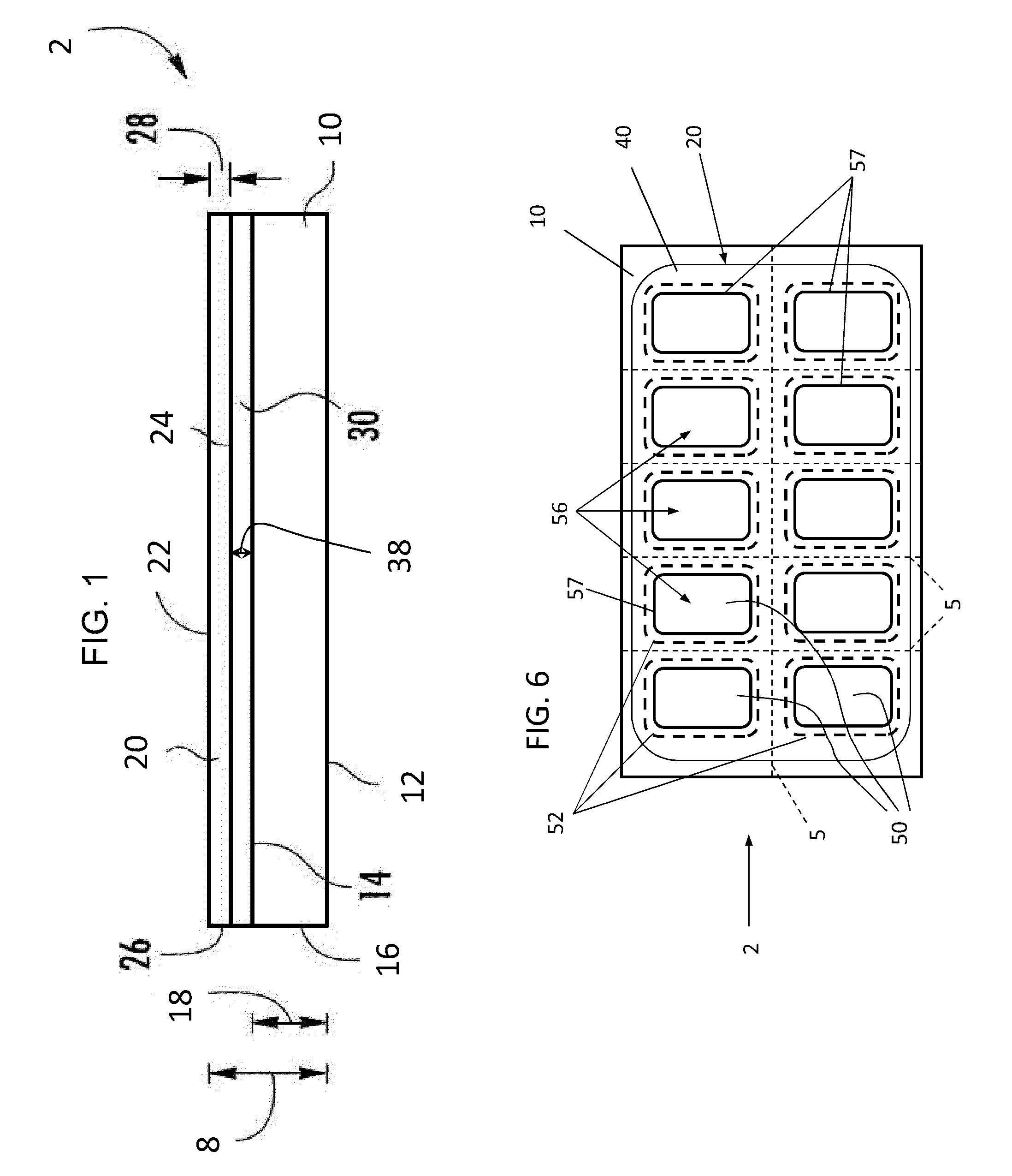
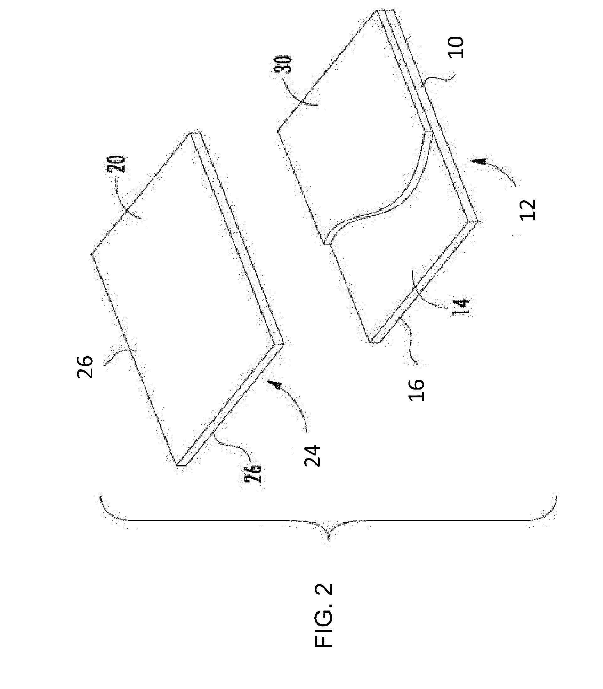
[0013]In light of the above, there is a need for a thin sheet-carrier article that can withstand the rigors of the FPD processing, including high temperature processing (without outgassing that would be incompatible with the semiconductor or display making processes in which it will be used), yet allow the entire area of the thin sheet to be removed (either all at once, or in sections) from the carrier so as to allow the reuse of the carrier for processing another thin sheet. The present specification describes ways to control the adhesion between the carrier and thin sheet to create a temporary bond sufficiently strong to survive FPD processing (including LTPS processing) but weak enough to permit debonding of the sheet from the carrier, even after high-temperature processing. Such controlled bonding can be utilized to create an article having a re-usable carrier, or alternately an article having patterned areas of controlled bonding and covalent bonding between a carrier and a sheet. More specifically, the present disclosure provides surface modification layers (including various materials and associated surface heat treatments), that may be provided on the thin sheet, the carrier, or both, to control both room-temperature van der Waals, and / or hydrogen, bonding and high temperature covalent bonding between the thin sheet and carrier. Even more specifically, the room-temperature bonding may be controlled so as to be sufficient to hold the thin sheet and carrier together during vacuum processing, wet processing, and / or ultrasonic cleaning processing. And at the same time, the high temperature covalent bonding may be controlled so as to prevent a permanent bond between the thin sheet and carrier during high temperature processing, as well as maintain a sufficient bond to prevent delamination during high temperature processing. In alternative embodiments, the surface modification layers may be used to create various controlled bonding areas (wherein the carrier and sheet remain sufficiently bonded through various processes, including vacuum processing, wet processing, and / or ultrasonic cleaning processing), together with covalent bonding regions to provide for further processing options, for example, maintaining hermeticity between the carrier and sheet even after dicing the article into smaller pieces for additional device processing. Still further, some surface modification layers provide control of the bonding between the carrier and sheet while, at the same time, reduce outgassing emissions during the harsh conditions in an FPD (for example LTPS) processing environment, including high temperature and / or vacuum processing, for example.

Problems solved by technology

However, the technology, equipment, and processes required for roll-to-roll processing of high quality displays are not yet fully developed.
The upper temperature limit of the PEN limits the device quality and process that can be used.
In addition, the high permeability of the polymer substrate leads to environmental degradation of OLED devices where a near hermetic package is required.
Thin film encapsulation offers the promise to overcome this limitation, but it has not yet been demonstrated to offer acceptable yields at large volumes.
The large thickness of these layers creates the potential for large amounts of volatiles, trapped solvents, and adsorbed species to contaminate FPD processes.
These materials thermally decompose and outgas above ˜250° C. The materials also may cause contamination in downstream steps by acting as a sink for gases, solvents and acids which can outgas in subsequent processes.
These conditions limit the materials that may be used, and place high demands on the carrier / thin sheet.
Prying or peeling cannot be used to separate the covalently bonded portion of the thin glass from the carrier and, thus, the entire thin sheet cannot be removed from the carrier.

Method used


Image

  • Methods for processing OLED devices
  • Methods for processing OLED devices
  • Methods for processing OLED devices

Examples


example 4a

[0076]A glass carrier with its bonding surface O2 plasma and SC1 treated was then treated with 1% dodecyltriethoxysilane (DDTS) in toluene, and annealed at 150° C. in vacuum for 1 hr to complete condensation. DDTS treated surfaces exhibit a surface energy of 45 mJ / m2. As shown in Table 4, a glass thin sheet (having been SC1 cleaned and heated at 400° C. in a vacuum for one hour) was bonded to the carrier bonding surface having the DDTS surface modification layer thereon. This article survived wet and vacuum process tests but did not survive thermal processes over 400° C. without bubbles forming under the carrier due to thermal decomposition of the silane. This thermal decomposition is expected for all linear alkoxy and chloro alkylsilanes R1xSi(OR2)y(Cl)z where x=1 to 3, and y+z=4−x except for methyl, dimethyl, and trimethyl silane (x=1 to 3, R1=CH3) which produce coatings of good thermal stability.

example 4b

[0077]A glass carrier with its bonding surface O2 plasma and SC1 treated was then treated with 1% 3,3,3, trifluoropropyltritheoxysilane (TFTS) in toluene, and annealed at 150° C. in vacuum for 1 hr to complete condensation. TFTS treated surfaces exhibit a surface energy of 47 mJ / m2. As shown in Table 4, a glass thin sheet (having been SC1 cleaned and then heated at 400° C. in a vacuum for one hour) was bonded to the carrier bonding surface having the TFTS surface modification layer thereon. This article survived the vacuum, SRD, and 400° C. process tests without permanent bonding of the glass thin sheet to the glass carrier. However, the 600° C. test produced bubbles forming under the carrier due to thermal decomposition of the silane. This was not unexpected because of the limited thermal stability of the propyl group. Although this sample failed the 600° C. test due to the bubbling, the material and heat treatment of this example may be used for some applications wherein bubbles a...

example 4c

[0078]A glass carrier with its bonding surface O2 plasma and SC1 treated was then treated with 1% phenyltriethoxysilane (PTS) in toluene, and annealed at 200° C. in vacuum for 1 hr to complete condensation. PTS treated surfaces exhibit a surface energy of 54 mJ / m2. As shown in Table 4, a glass thin sheet (having been SC1 cleaned and then heated at 400° C. in a vacuum for one hour) was bonded to the carrier bonding surface having the PTS surface modification layer. This article survived the vacuum, SRD, and thermal processes up to 600° C. without permanent bonding of the glass thin sheet with the glass carrier.


PUM

PropertyMeasurementUnit
temperatureaaaaaaaaaa

Abstract

Methods for making electronic devices on thin sheets bonded to carriers. A surface modification layer and associated heat treatments, may be provided on a sheet, a carrier, or both, to control both room-temperature van der Waals (and/or hydrogen) bonding and high temperature covalent bonding between the thin sheet and carrier during the electronic device processing. The room-temperature bonding is controlled so as to be sufficient to hold the thin sheet and carrier together during vacuum processing, wet processing, and/or ultrasonic cleaning processing, during the electronic device processing. And at the same time, the high temperature covalent bonding is controlled so as to prevent a permanent bond between the thin sheet and carrier during high temperature processing, during the electronic device processing, as well as maintain a sufficient bond to prevent delamination during high temperature processing.

Description

[0001]This application claims the benefit of priority under 35 U.S.C. §119 of U.S. Provisional Application Ser. No. 61 / 736,871, filed on Dec. 13, 2012, the content of which is relied upon and incorporated herein by reference in its entirety.BACKGROUND[0002]1. Field of the Invention[0003]The present invention is directed to articles and methods for processing electronic devices on flexible sheets on carriers and, more particularly to articles and methods for processing electronic devices on flexible glass sheets on glass carriers.[0004]2. Technical Background[0005]Flexible substrates offer the promise of cheaper devices using roll-to-roll processing, and the potential to make thinner, lighter, more flexible and durable displays. However, the technology, equipment, and processes required for roll-to-roll processing of high quality displays are not yet fully developed. Since panel makers have already heavily invested in toolsets to process large sheets of glass, laminating a flexible s...

Claims


Application Information

Patent Timeline
Patent Type & Authority Applications(United States)
IPC IPC(8): H01L51/00
CPCY02E10/549Y10T156/10Y10T156/1052H01L21/2007Y02P70/50H10K71/80H10K77/111H10K59/1201H10K2102/311
Inventor BELLMAN, ROBERT ALANBOOKBINDER, DANA CRAIGMANLEY, ROBERT GEORGEMAZUMDER, PRANTIK
Owner CORNING INC
Why Eureka
Try Eureka