Multi-frequency clock skew control for inter-chip communication in synchronous digital systems

Active Publication Date: 2014-06-19
COHERENT LOGIX
View PDF3 Cites 13 Cited by
  • Summary
  • Abstract
  • Description
  • Claims
  • Application Information

AI Technical Summary

Benefits of technology

The patent describes a method and system for reconfiguring clock generation circuitry in a synchronous digital system. This allows for the replacement of a primary clock without causing errors in the system. The system can select between multiple clock signals and change settings or power down / up the circuitry to minimize clock skew and ensure accurate synchronization. The technical effects include improved reliability and flexibility in clock signal selection and minimization of clock skew.

Problems solved by technology

For large, expensive computer systems, their economics dictates that they be kept busy all the time.
For small, inexpensive computers, continuous high speed operation is not required, and is even a hindrance for battery operated devices.
While there are entertainment applications that require high performance operation for hours at a time, most uses of small computers require bursts of high performance for less than a minute.
However reduced system clock frequency (or rate) also slows the resident kernel of the operating system software and its response time.
If a processor's power is completely cut off the data in its volatile memory is lost; and upon re-activation of the processor, data will have to be reloaded from non-volatile memory.
If a user is editing video there may be frequent pauses in the display of motion.
If the transmitter temporarily has no new data to send, the receiver may erroneously keep reading the last bit of data unless it gets a not-ready signal from the transmitter.
Similarly, if the receiver temporarily has no place to put data, it may erroneously ignore arriving data unless it can tell the transmitter to stop sending.
Clock frequencies this high are reasonable inside an IC where wires are physically short, but are difficult to manage for the chip I / O and inter-chip links.
For a processor and memory, turning power back on and resuming processing is much more complicated than turning it off.
At very low frequencies there is a power floor where the dc leakage currents will dominate the overall power consumption.
At very high frequencies the transistors are not fast enough to completely switch the signal lines, and this causes bit errors and excess supply current.
Often the bit errors can be suppressed by increasing the V of the supply but this causes a quadratic increase in power until the circuits are damaged by overheating.
Level shifting circuits are well known in the industry, and easily added, but they may introduce additional power dissipation and signal delay.
The disadvantage of this tree compared the H tree is that the central area has a clock signal that is skewed (phase advanced) in steps with respect to the perimeter of the chip.
If the counter is excessively long (to cover a wider range of frequencies) it begins to take up excess silicon real-estate and adds to leakage power dissipation.
However, at high clock rates it is difficult to align the phase of the inter-chip sync signals to properly reset CNT0, which is running on a clock phase locked to CLKREF.
However, this limits the speed of the PEs and DMRs in the core of the chip and thus the range of applications.
Flow control between the I / O cell and the DMR prevents data loss or duplication; however, a data jam may result if a slowed I / O cell is sent data at a higher rate than it can process.

Method used


Image

  • Multi-frequency clock skew control for inter-chip communication in synchronous digital systems
  • Multi-frequency clock skew control for inter-chip communication in synchronous digital systems
  • Multi-frequency clock skew control for inter-chip communication in synchronous digital systems

Examples


Embodiment Construction

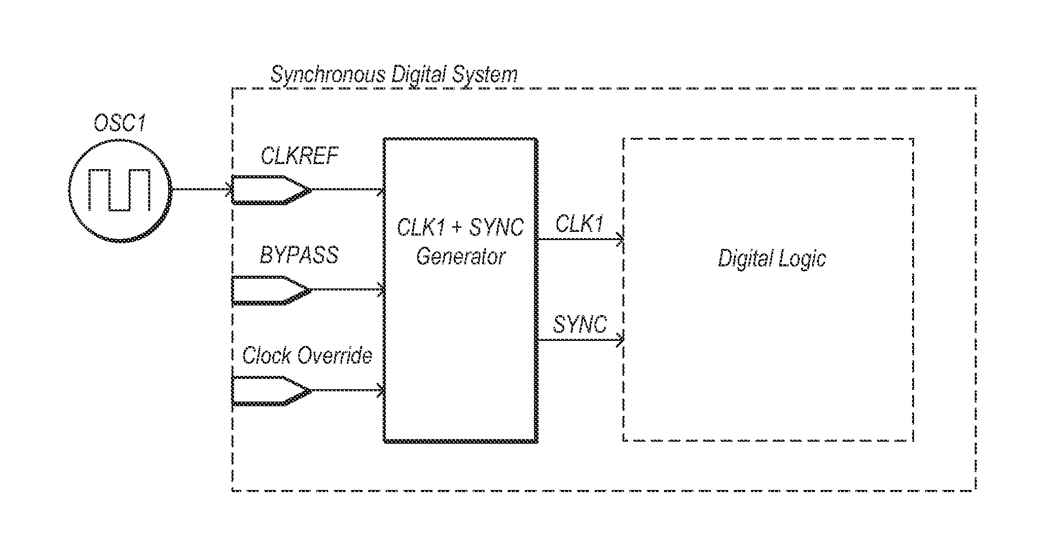
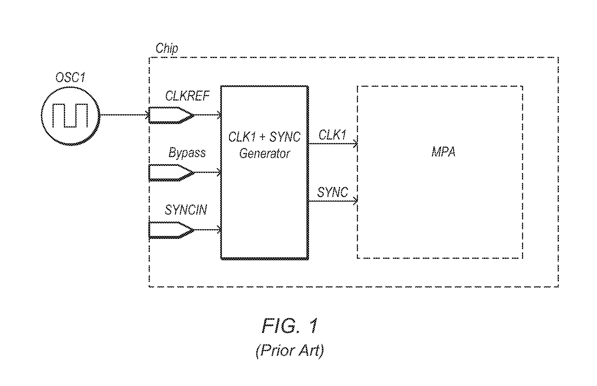
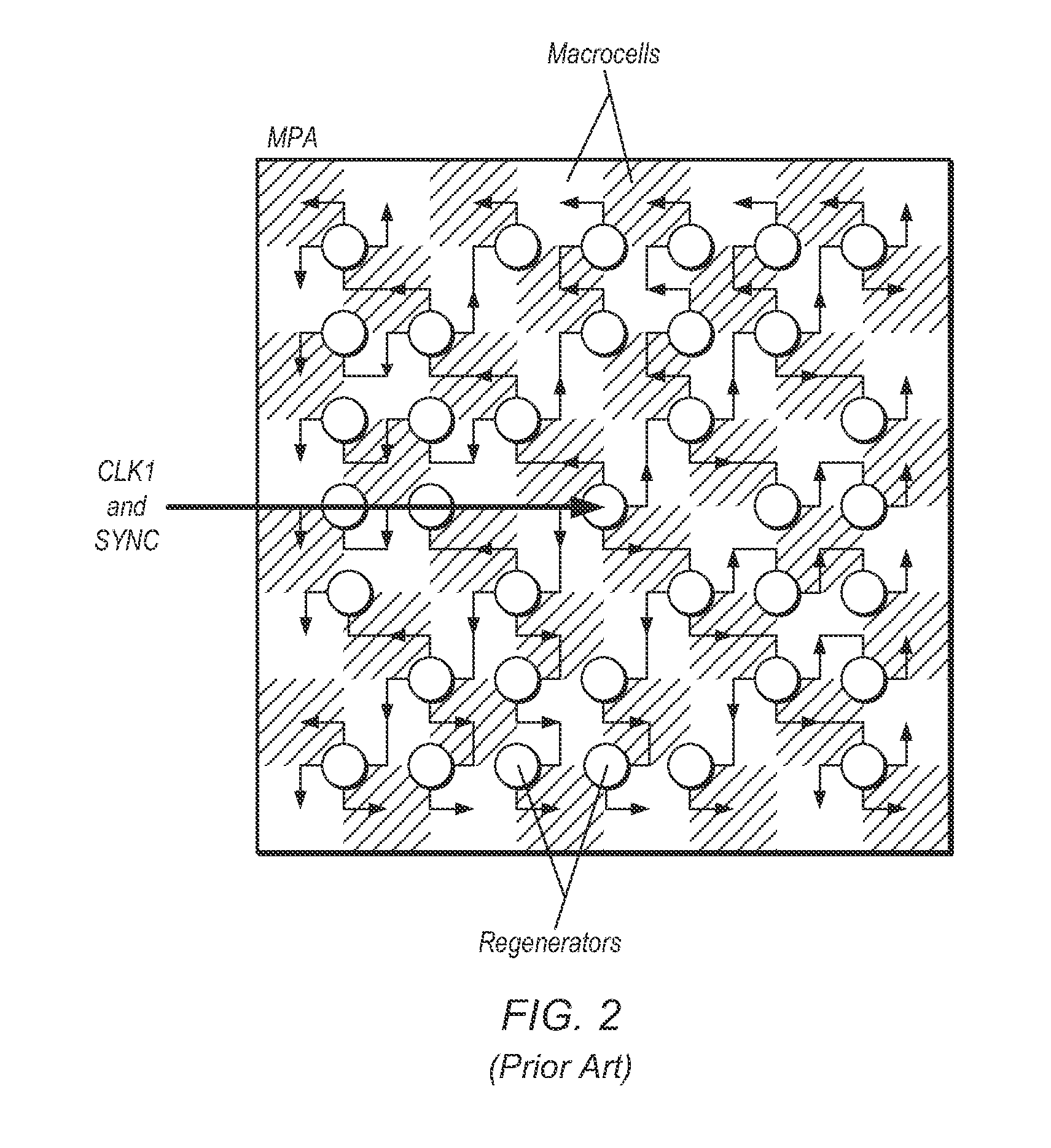
[0062]Various embodiments of methods and circuits are disclosed, in which clock and select signals may be distributed throughout a synchronous digital system.

[0063]In one embodiment, a method is disclosed for reconfiguring clock generation circuitry in a clock distribution network of a synchronous digital system. A first clock signal may be generated and selected as a primary clock. A second clock signal may then replace the first clock as the primary clock, without causing clock-induced errors in the synchronous digital system. The clock generation circuitry may then be reconfigured during the time that the second clock signal is acting as the primary clock. The first clock signal may then be selected again as the primary clock, after the clock generation circuitry has stabilized, without causing clock-induced errors in the synchronous digital system.

[0064]In some embodiments, the second clock signal may be an external clock signal. In other embodiments, in which the synchronous di...


PUM


Abstract

Embodiments are disclosed of a multi-chip apparatus capable of performing multi-rate synchronous communication between component chips. Each chip may receive a common clock reference signal, and may generate an internal clock signal dependent on the clock reference signal. A clock distribution tree and phase-locked loop may be used to minimize internal clock skew at I / O circuitry at the chip perimeter. Each chip may also generate an internal synchronizing signal that is phase-aligned to the received clock reference signal. Each chip may use its respective synchronizing signal to synchronize multiple clock dividers that provide software-selectable reduced-frequency clock signals to the I / O cells of the chip. In this way, the reduced-frequency clock signals of the multiple chips are edge-aligned to the low-skew internal clock signals, and phase-aligned to the common clock reference signal, allowing the I / O cells of the multiple chips to perform synchronous communication at multiple rates with low clock skew.

Description

PRIORITY CLAIM[0001]The present application claims benefit of priority of provisional application Ser. No. 61 / 736,763 titled “Clock Distribution Network for Multi-Frequency Multi-Processor Systems” and filed on Dec. 13, 2012, which is hereby incorporated by reference in its entirety as though fully and completely set forth herein.BACKGROUND[0002]1. Technical Field[0003]This application relates to electronic systems and, more particularly, to clock signal distribution networks within digital electronic systems, and especially to clock distribution within integrated circuit (IC) chips that contain many processing units.[0004]2. Description of the Related Art[0005]For large, expensive computer systems, their economics dictates that they be kept busy all the time. Performance was traditionally measured as computations per second. For small, inexpensive computers, continuous high speed operation is not required, and is even a hindrance for battery operated devices. Increasingly computer ...

Claims


Application Information

Patent Timeline
IPC IPC(8): H03L7/08
CPCG06F1/04G06F1/08G06F1/10G06F1/324G06F11/1604H03L7/06Y02D10/00H03K3/0315H03L7/08H03L7/085
Inventor DOBBS, CARL S.TROCINO, MICHAEL R.FAULKNER, KENNETH R.SCHREPPEL, CHRISTOPHER L.
Owner COHERENT LOGIX
Why Eureka
Try Eureka