

Semiconductor device and method for manufacturing the same
- Summary
- Abstract
- Description
- Claims
- Application Information
AI Technical Summary
Benefits of technology
Problems solved by technology
Method used
Image

Examples
embodiment 1
[0083]In this embodiment, a semiconductor device of one embodiment of the present invention is described with reference to drawings.
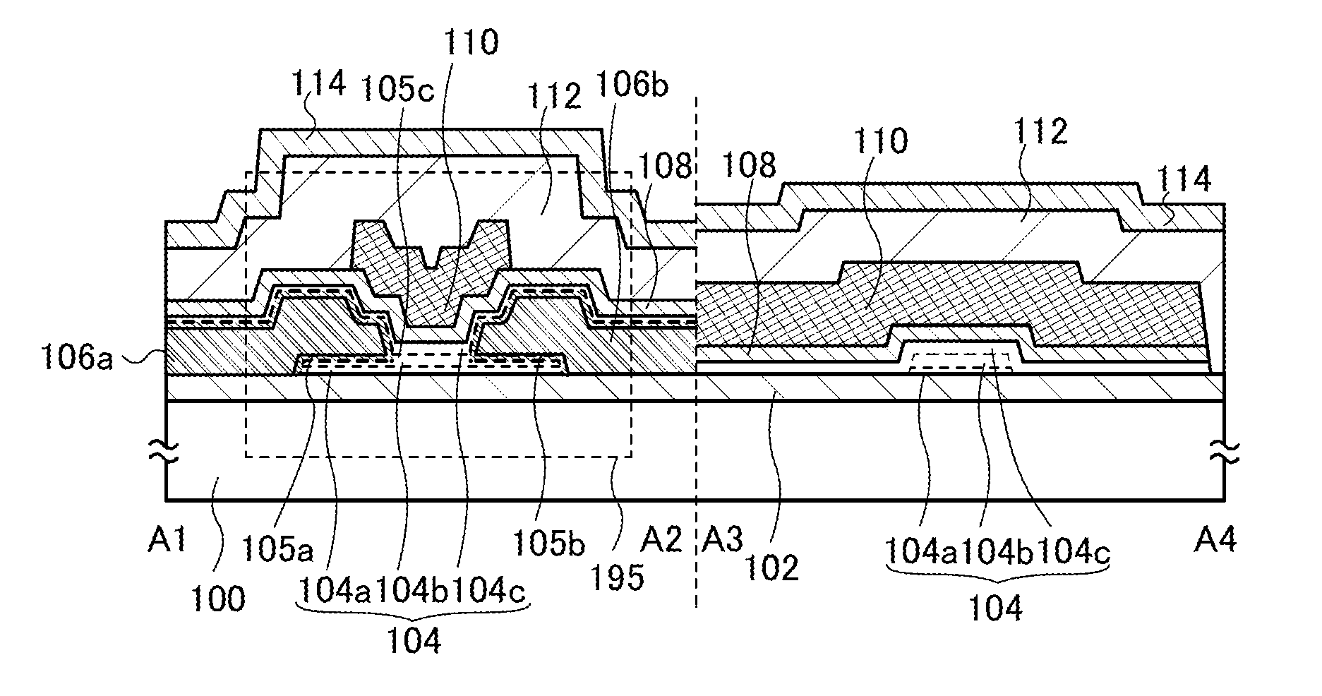
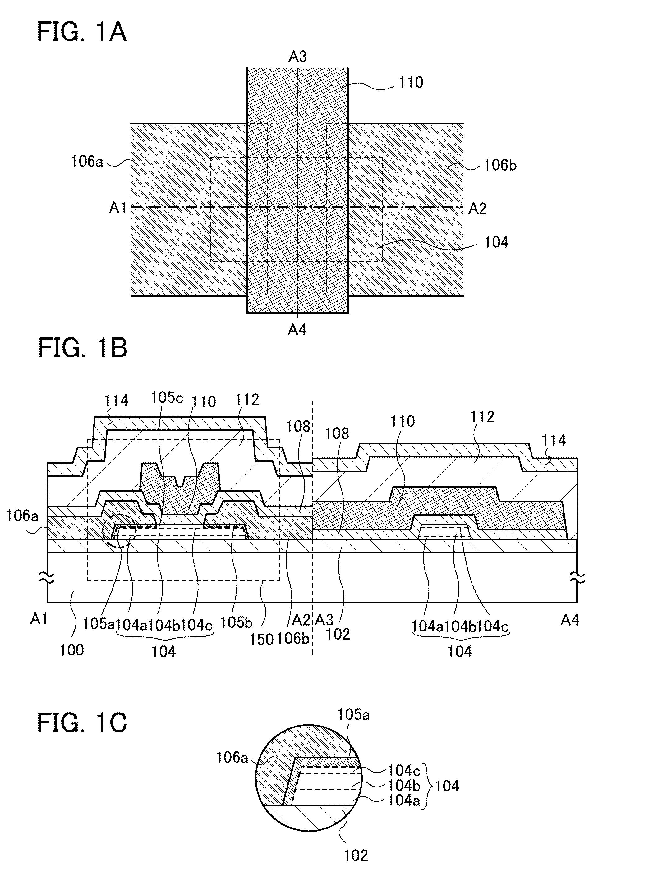
[0084]FIGS. 1A to 1C are a top view and cross-sectional views illustrating a transistor of one embodiment of the present invention. FIG. 1A is the top view, and a cross section taken along a dashed-dotted line A1-A2 and a dashed-dotted line A3-A4 in FIG. 1A corresponds to FIG. 1B. FIG. 1C is an enlarged view of a region surrounded by a circle of a dotted line in FIG. 1B. Note that some components in the top view in FIG. 1A are not illustrated for simplification of the drawing.
[0085]A transistor 150 illustrated in FIGS. 1A to 1C includes a base insulating film 102 over a substrate 100; a multilayer film 104 including an oxide semiconductor film over the base insulating film 102; a low-resistance region 105a and a low-resistance region 105b over the multilayer film 104; a source electrode 106a over the low-resistance region 105a; a drain electrode 106b ov...
embodiment 2
[0208]In this embodiment, a method for manufacturing the transistor 150 described in Embodiment 1 with reference to FIGS. 1A to 1C is described.
[0209]First, the base insulating film 102 is formed over the substrate 100.
[0210]A glass substrate, a ceramic substrate, a quartz substrate, a sapphire substrate, or the like can be used as the substrate 100. Alternatively, a single crystal semiconductor substrate or a polycrystalline semiconductor substrate made of silicon, silicon carbide, or the like, a compound semiconductor substrate made of silicon germanium or the like, a silicon-on-insulator (SOI) substrate, or the like may be used. Still alternatively, any of these substrates further provided with a semiconductor element may be used.
[0211]The base insulating film 102 can be formed by a plasma chemical vapor deposition (CVD) method, a sputtering method, or the like using an oxide insulating film of aluminum oxide, magnesium oxide, silicon oxide, silicon oxynitride, gallium oxide, ger...
embodiment 3
[0297]In this embodiment, a transistor having a structure different from that of the transistor described in Embodiment 1 is described.
[0298]FIGS. 10A to 10C are a top view and cross-sectional views of a transistor of one embodiment of the present invention. FIG. 10A is a top view, and a cross section taken along a dashed-dotted line B1-B2 and a dashed-dotted line B3-B4 in FIG. 10A is illustrated in FIG. 10B. FIG. 10C is an enlarged view of a region surrounded by a dashed-line circle in FIG. 10B. Note that for simplification of the drawing, some components in the top view in FIG. 10A are not illustrated.
[0299]A transistor 250 illustrated in FIGS. 10A to 10C includes: the gate electrode 110 over the substrate 100; the gate insulating film 108 over the gate electrode 110; the multilayer film 104 over the gate insulating film 108; the low-resistance region 105a and the low-resistance region 105b over the multilayer film 104; the source electrode 106a over the low-resistance region 105a...
PUM
 Abstract
Description
Claims
Application Information