

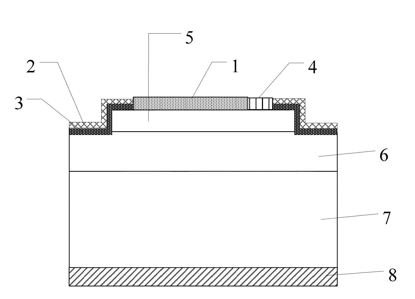
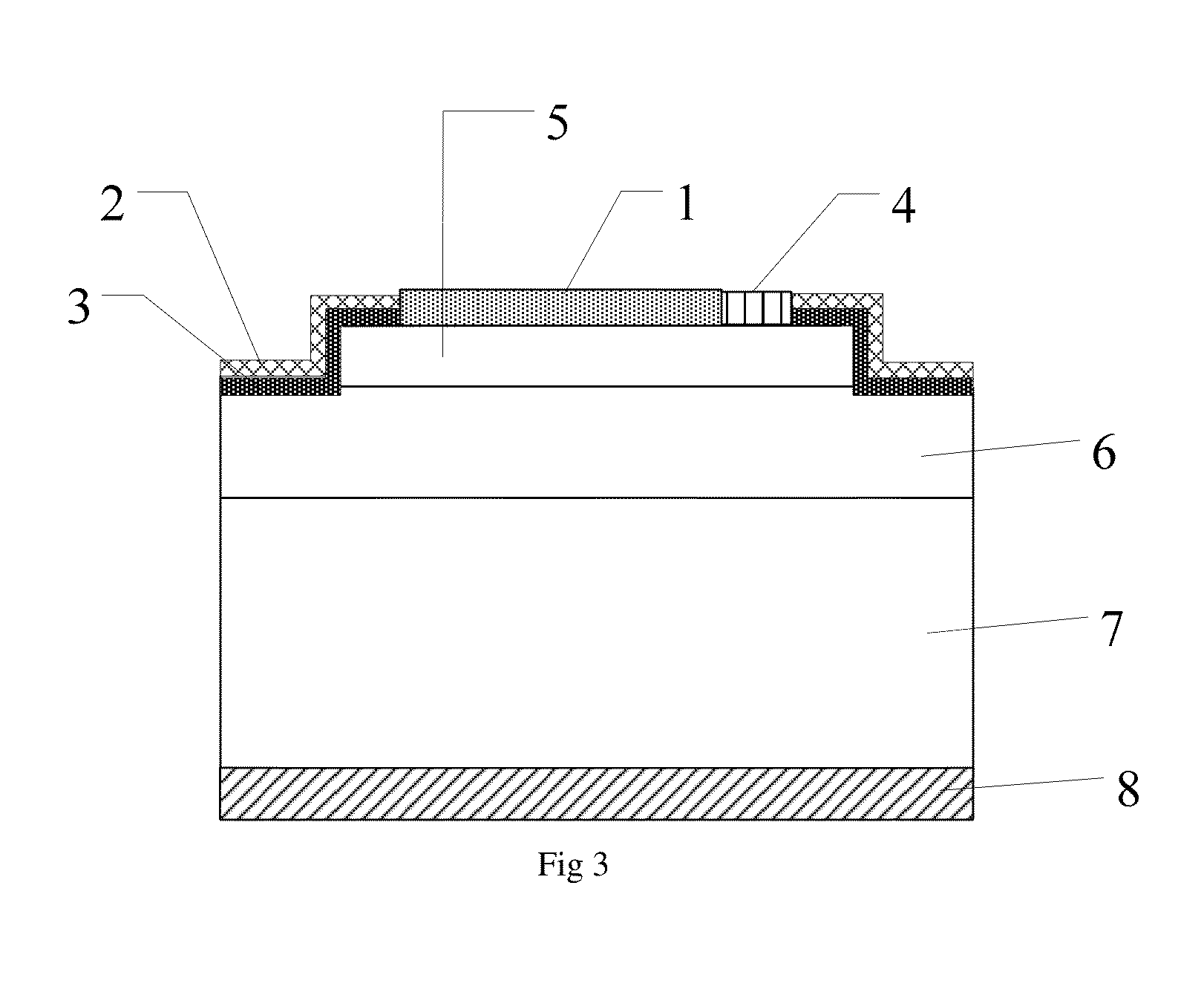
I-Layer Vanadium-Doped Pin Type Nuclear Battery and the Preparation Process Thereof
a technology of i-layer vanadium and pin type, applied in the field of microelectronic technology, can solve the problems of increasing the leakage current of the device, low energy conversion, and large loss of injecting particles, so as to improve the collection ratio of the generated electron-hole pair, reduce the concentration of i-layer carriers, and increase the width of depletion area
- Summary
- Abstract
- Description
- Claims
- Application Information
AI Technical Summary
Benefits of technology
Problems solved by technology
Method used
Image

Examples
example 2
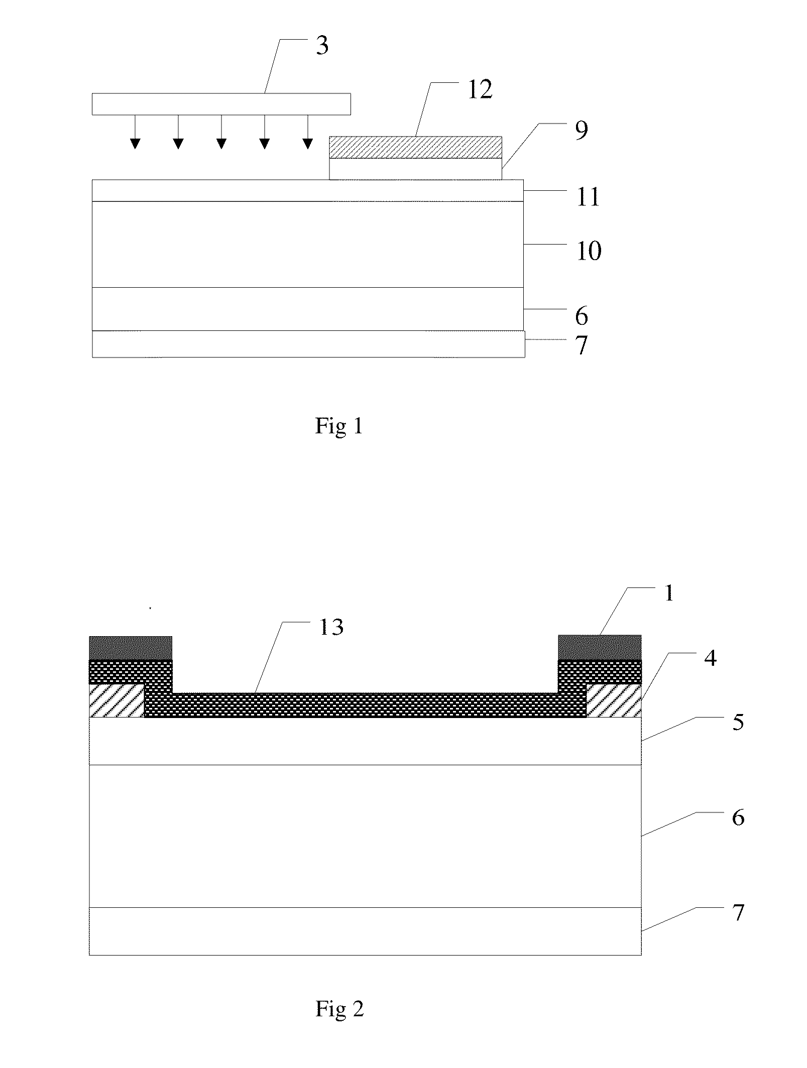
[0065]Step 1: an n-type epitaxial layer was epitaxially grown on a high doping n-type SiC substrate, shown as in FIG. 4a.
[0066]A high doping n-type SiC substrate 7 with a doping concentration of 5×1018 cm−3 was selected, after cleaning, an original n-type epitaxial layer doped with nitrogen ions with a thickness of 3 μm was epitaxially grown on the high doping n-type SiC substrate, the doping concentration was 5×1015 cm−3, and the epitaxial temperature was 1570° C., the pressure was 100 mbar, and the reacted gases were silane and propane, the carrier gas was pure hydrogen, and the impurity source was liquid nitrogen.
[0067]Step 2: vanadium ions were injected into the original n-type SiC epitaxial layer with a doping concentration of 5×1015 cm−3, as shown in FIG. 4b.
[0068](2.1) vanadium ions were injected into the original n-type SiC epitaxial layer with a doping concentration of 5×1015 cm−3, the injecting condition was that the injecting energy of said vanadium ions was 2000 KeV, a...
example 3
[0087]Step A: an n-type epitaxial layer was epitaxially grown on a high doping n-type SiC substrate, shown as in FIG. 4a.
[0088]A high doping n-type SiC substrate 7 with a doping concentration of 7×1018 cm−3 was selected, after cleaning, an original n-type epitaxial layer doped with nitrogen ions with a thickness of 5 μm was epitaxially grown on the high doping n-type SiC substrate, the doping concentration was 2×1015 cm−3, and the epitaxial temperature was 1570° C., the pressure was 100 mbar, and the reacted gases were silane and propane, the carrier gas was pure hydrogen, and the impurity source was liquid nitrogen.
[0089]Step B: vanadium ions were injected into the original n-type SiC epitaxial layer with a doping concentration of 2×1015 cm−3, as shown in FIG. 4b.
[0090](B1) vanadium ions were injected into the original n-type SiC epitaxial layer with a doping concentration of 2×1015 cm−3, the injecting condition was that the injecting energy of said vanadium ions was 2500 KeV, an...
PUM
| Property | Measurement | Unit |
|---|---|---|
| thickness | aaaaa | aaaaa |
| thickness | aaaaa | aaaaa |
| thickness | aaaaa | aaaaa |
Abstract
Description
Claims
Application Information