Bright source protection for low light imaging sensors

a low-light imaging and bright source protection technology, applied in the field of low-light imaging sensors, can solve the problems of permanent damage marks on the detector material of the sensor, complete loss of contrast, and degradation of performance, and achieve the effect of reducing ion damage to the photo-cathode, increasing the sensitivity of the i2 tube, and not needing to reduce the voltage across the mcp

Inactive Publication Date: 2014-08-28
THE SEC OF STATE FOR DEFENCE IN HER BRITANNIC MAJESTYS GOVERNMENT OF THE UK OF GREAT BRITAIN & NORTHERN IRELAND
View PDF1 Cites 13 Cited by
  • Summary
  • Abstract
  • Description
  • Claims
  • Application Information

AI Technical Summary

Benefits of technology

[0011]Instead of spectrally limiting the light incident onto the photo-cathode through filters placed beforehand, it is possible to spatially limit light from areas of the scene where the sources are located. This requires protection measures that are located at a focal plane of the imaging system, i.e. at an intermediate focal plane or at the detector material to spatially limit the generation or subsequent diffusion of electrons in the photo cathode material. Spatial protection effectively blocks out areas of the image where bright sources are located whilst allowing low intensity light from other areas of the scene to pass and form an image on the detector.
[0013]The introduction of a photo-sensitive layer (PSL), positioned in between a transparent electrode and the photo cathode allows localised photo-generated charge to move from the photo-cathode through the PSL and onto the transparent electrode under the action of an applied field. The movement of photo-generated charge occurs locally in areas of the focal plane where relatively high irradiances are seen from a bright light source in the scene. Therefore the provision of a photo-sensitive material layer into the design of an image intensification tube affords the device spatial bright source protection (BSP) without compromising the optical intensification in low light areas of the scene. Spatial BSP can be realised through this use of the photo-sensitive material layer that, upon illumination, provides a method of locally limiting the number of, or the subsequent diffusion of the photo-generated electrons within the photo-cathode. The advantage of a night vision device employing an I2 tube with spatial BSP is to allow the device to operate as normal for low light areas of the scene, retaining image contrast and scene situational awareness should an intense light source be directed towards the device. By spatially limiting the electron emission from the photo-cathode under intense illumination the photo-cathode does not need to be power limited by traditional BSP electronics, thereby allowing normal operation under the bright conditions so that the operators' spatial acuity and contrast sensitivity are not affected. Where the electron receiving device is a MCP, the lifetime of the I2 tube will be extended through the reduction of ion damage to the photo-cathode caused by the excesses of emitted electrons from the photo-cathode incident on the MCP. This also removes the need for an ion absorbing thin film, which allows the increased sensitivity of the I2 tube. Furthermore, the voltage across the MCP does not need to be reduced due to increasing brightness levels thereby allowing the tube to continue to operate under normal gain conditions, increasing image contrast for the dark areas of the scene and reducing the chance of dazzle and the size of any halo effects. Additional benefits of the inclusion of a photo-sensitive layer are also realised. A variable degree of control over the voltage applied across the photo-sensitive layer and the photo-cathode adds the benefit that the amount of spatial protection can be easily adjusted, possibly in response to increasing current drawn by the photo-cathode. Reversing the polarity of the applied voltage also improves sensor dynamic range in extremely dark conditions. Upon leaving the back surface of the MCP the electronic image can be converted into a visible image through the fluorescence of the phosphor brought on by electron, bombardment of an aluminised phosphor coating or phosphor screen.
[0014]Optionally placing the photo-cathode material in proximity focus with an active pixel sensor, such as a high resolution complementary metal oxide semiconductor (CMOS) chip anode. The electrons emitted by the photo-cathode will be directly injected in the electron receiving mode into the CMOS anode. Here the electrons are collected, amplified and read out to produce a direct digital video output that can be viewed by the user in any number of ways. The advantage of using an electron receiving device such as a CMOS chip is that the vision sensor can be used in ambient light conditions such as dusk or daylight.
[0015]When a layer of dielectric material is positioned between the photo-cathode and PSL, the dielectric material electrically separates the PSL and photo-cathode layers. In this scheme the intention is to create a surface potential at the front of the photo cathode material (i.e. GaAs) and a depletion region within the bulk material of the photo cathode. In bright areas of the image an applied field placed across the electrode and the photo-cathode creates this surface potential and influences the diffusion of photo generated electrons in the photo-cathode. The influence on the diffusion electrons in the bulk semi-conductor material is in the opposite direction of the photo-cathode's emission surface. If a MCP is used as the electron receiving device, the overall probability of escape and amplification at the MCP reduces and therefore damaging effects to the MCP are reduced. This influence only happens in areas of the focal plane where relatively high irradiances are seen from a bright light source in the scene.

Problems solved by technology

I2 tubes for night vision devices, when operated in the presence of high intensity light sources, often have degraded performance due to optical effects like blooming, halo and loss of image contrast through automatic gain control.
High intensity light sources such as display screens, street lights, welding arcs or car head lamps, can also lead to complete loss of contrast and the creation of permanent damage marks on the detector material of the sensor.
These effects cause degradation of image quality or loss of situational awareness for the user rendering them unusable in their intended role.
There also exists high potential differences between the front and rear faces of the MCP and between the rear face of the MCP and the aluminised phosphor screen.
In many cases over-exposure to bright light sources can directly lead to permanent ‘scarring’ of the photo-cathode material.
Prolonged exposure can cause burn marks to appear on the photo-cathode.
This damage is caused by impurity ions, generally potassium, transferred from the MCP to the photo-cathode resulting in regions of low sensitivity and even permanent black scarring corresponding to the bright regions of the scene; this is caused by the bombardment and sputtering of the activation surface of the photo-cathode.
Even so these films almost certainly let through large numbers of ions and more often the tube is taken out of service due to its reduced performance.
However, the effect of this is twofold; it is recognised that the reduction of the MCP voltage results in the appearance of fixed pattern noise (the matrix pattern of the MCP) in the image and it is also observed that contrast in non-bright areas of the image is lost due to the reduction in gain; an effect known as ‘dazzle’.
Blooming and dazzle are common problems for intensification devices; as such bright sources are a significant problem for the use of night vision equipment.
However the limitation of light incident onto the photo-cathode of an image intensification tube inherently degrades the performance of the device and restricts its operational envelope.
Therefore intensification tube manufacturers do not incorporate EOPM into tube technology.
However, the performance of a reflecting filter is highly dependent on the incident direction and the incident wavelength and to employ such a laser protective filter the manufacturers must have some knowledge about the laser source, which is not always available.
Although it is possible to make a reflecting filter that provides the high optical rejection needed to protect an image intensifier, adequately suppressing off-axis light is a real problem for the filter design.
Furthermore reflecting filters are expensive and the potential for detection of the reflected signal is a further disadvantage in certain applications.
Although protection from blooming, dazzle and damage at key wavelengths can easily be achieved, the methods are limited in their application through the amount of optical loss they cause the device.
Key wavelength protection cannot afford the same protection for broadband light sources owing to the wavelength bandwidth of the source—successive implementation of multiple interfering or absorbing filters to protect from several key wavelengths will introduce an optical loss that cannot be tolerated by the user of the sensor.

Method used


Image

  • Bright source protection for low light imaging sensors
  • Bright source protection for low light imaging sensors
  • Bright source protection for low light imaging sensors

Examples


first embodiment

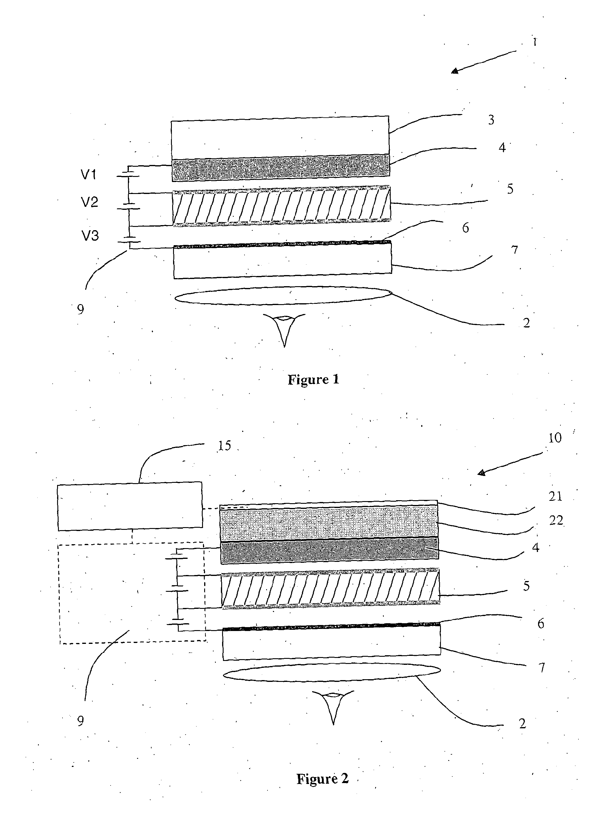
[0019]FIG. 2 is an example layout of an intensification tube according to the present invention;

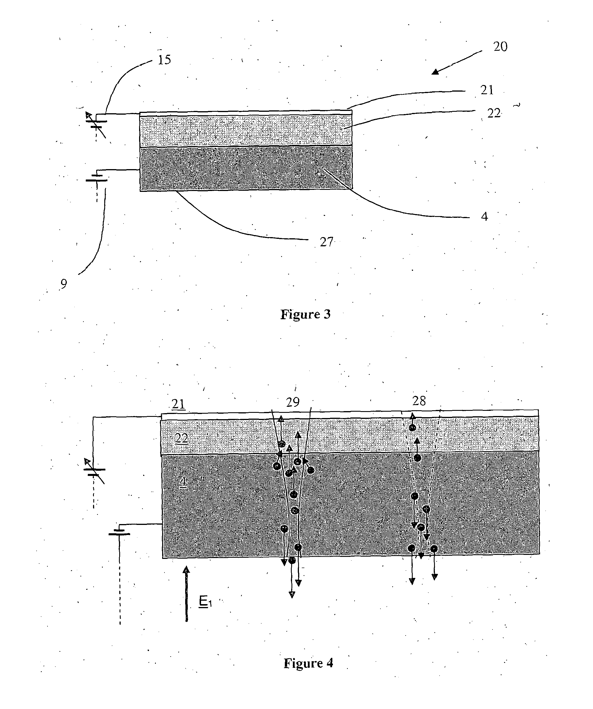
[0020]FIG. 3 illustrates part of the first embodiment of the invention;

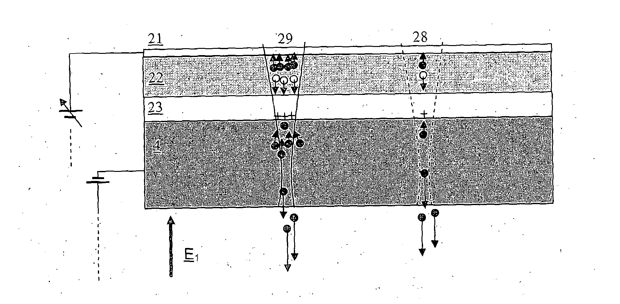
[0021]FIG. 4 is a sketch showing the action of the photo-generated electrons in the photo-cathode and photo-sensitive layer under the applied fields in low and high intensity illumination cases for the first embodiment of the present invention;

second embodiment

[0022]FIG. 5 is an example layout of an intensification tube according to the present invention;

[0023]FIG. 6 illustrates part of the second embodiment of the present invention;

[0024]FIG. 7 is a sketch showing the action of the photo-generated electrons in the photo-cathode, photo-sensitive layer and dielectric materials under the applied fields in low and high intensity illumination cases for the second embodiment of the present invention.

third embodiment

[0025]FIG. 8 is an example layout of an electron receiving silicon image chip according to the present invention;

[0026]FIG. 9 is an example layout of an electron receiving silicon image chip with an additional insulating layer according to a forth embodiment of the present invention;


PUM


Abstract

This invention relates to a low light imaging sensors and particularly image intensification and CMOS sensors. To overcome issues of dazzle and halo when operating in areas where the scene encompasses bright light sources, the invention provides material layers in contact with the detector material to spatially limit the generation or subsequent diffusion of electrons in said detector material. This allows the imaging sensor to perform as normal under bright conditions, maintaining the operator's scene awareness and spatial acuity.

Description

TECHNICAL FIELD OF THE INVENTION[0001]This invention relates to a low light imaging sensors and particularly image intensification and CMOS sensors.[0002]Most imaging sensors, which include Image Intensification (I2) technology, operate by converting an optical image into an electrical signal, which is then amplified and then reconverted back to a visible image. I2 tubes for night vision devices, when operated in the presence of high intensity light sources, often have degraded performance due to optical effects like blooming, halo and loss of image contrast through automatic gain control. High intensity light sources such as display screens, street lights, welding arcs or car head lamps, can also lead to complete loss of contrast and the creation of permanent damage marks on the detector material of the sensor. These effects cause degradation of image quality or loss of situational awareness for the user rendering them unusable in their intended role.[0003]In typical modem photo-ca...

Claims


Application Information

Patent Timeline
Patent Type & Authority Applications(United States)
IPC IPC(8): H01J40/16H01L27/146
CPCH01J40/16H01L27/14625H01J31/26H01J31/507H01J43/246G02B23/12H01J29/02H01J31/50H01J31/506
Inventor BURGESS, CHRISTOPHER DAVIDHILL, LEE
Owner THE SEC OF STATE FOR DEFENCE IN HER BRITANNIC MAJESTYS GOVERNMENT OF THE UK OF GREAT BRITAIN & NORTHERN IRELAND
Why Eureka
Try Eureka