Device architecture and method for temperature compensation of vertical field effect devices

a technology of vertical field effect and device architecture, which is applied in the direction of semiconductor/solid-state device manufacturing, semiconductor devices, electrical devices, etc., can solve the problems of thermal runaway of mosfet, increase of mosfet junction temperature, and further increase of resistance, so as to reduce the variation of rdson and reduce the temperature variation of resistance

Inactive Publication Date: 2014-09-18
D3 SEMICON
View PDF7 Cites 17 Cited by
  • Summary
  • Abstract
  • Description
  • Claims
  • Application Information

AI Technical Summary

Benefits of technology

[0006]The present disclosure is a field-effect device architecture that reduces the temperature variation of resistance. In...

Problems solved by technology

Power dissipation in turn causes the MOSFET junction temperature to increase, which further increases t...

Method used


Image

  • Device architecture and method for temperature compensation of vertical field effect devices
  • Device architecture and method for temperature compensation of vertical field effect devices
  • Device architecture and method for temperature compensation of vertical field effect devices

Examples


third embodiment

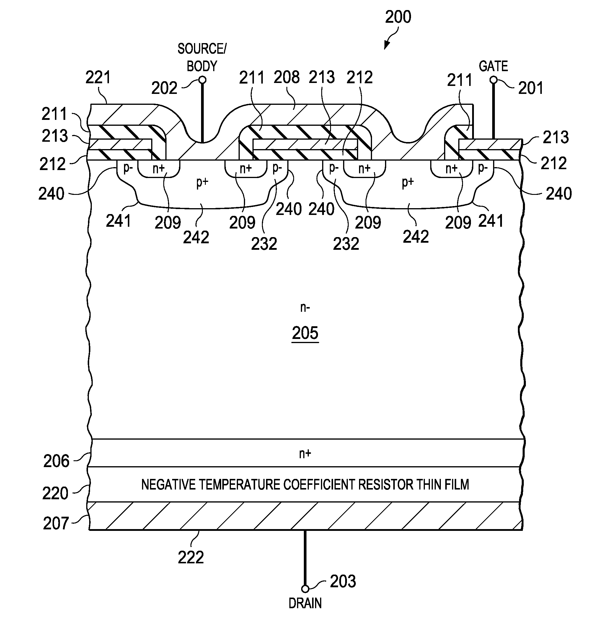
[0065]In a third embodiment, silicon-chromium is selected as the material of the resistive thin film. The silicon percentage of the silicon-chromium film is chosen in the range of 40% to 80% and the thin film is grown with a thickness in the range of approximately 25 A to approximately 2000 A as required to achieve the desired sheet resistance value for the resistive layer at the base temperature (such as 25° C.) and the desired temperature dependence curve.

fourth embodiment

[0066]In a fourth embodiment, silicon-nickel is selected as the material of the resistive thin film. The silicon percentage of the silicon-nickel film is chosen in the range of 40% to 80% and the thin film is grown with a thickness in the range of approximately 25 A to approximately 2000 A as required to achieve the specified resistance value for the resistive layer at the base temperature (such as 25° C.) and the desired temperature dependence curve.


PUM


Abstract

A field effect device is disclosed that provides a reduced variation in on-resistance as a function of junction temperature. The field effect device, having a source junction, gate junction and drain junction, includes a resistive thin film adjacent the drain junction wherein the resistive thin film comprises a material having a negative temperature coefficient of resistance. The material is selected from one or more materials from the group consisting of doped polysilicon, amorphous silicon, silicon-chromium and silicon-nickel, where the material properties, such as thickness and doping level, are chosen to create a desired resistance and temperature profile for the field effect device. Temperature variation of on-resistance for the disclosed field effect device is reduced from the temperature variation for a similar field effect device without the resistive thin film.

Description

CROSS-REFERENCE TO RELATED APPLICATION[0001]This application claims priority benefit from U.S. Provisional Application No. 61 / 778,698 filed Mar. 13, 2013. The patent application identified above is incorporated here by reference in its entirety to provide continuity of disclosure.FIELD OF THE INVENTION[0002]The present invention relates generally to the methods and techniques for reducing the temperature variation of resistance of a vertical MOSFET devices.BACKGROUND OF THE INVENTION[0003]For many years, manufacturers and developers of high performance power electronics have sought to improve power-handling density and manage device heat dissipation of discrete electronic components.[0004]Vertical MOSFETs have an on-resistance (“RdsOn”) that increases monotonically and super-linearly with temperature. As the on-resistance increases, so does the power dissipated for a given drain current (Id) according to the power equation: Power=Id2×RdsOn. Power dissipation in turn causes the MOSFE...

Claims


Application Information

Patent Timeline
IPC IPC(8): H01L29/78H01L29/66
CPCH01L29/66712H01L29/7803H01L23/367H01L29/0684H01L29/808H01L29/8083H01L29/04H01L29/0878
Inventor HARRINGTON, III, THOMAS E.
Owner D3 SEMICON
Why Eureka
Try Eureka