
Heated electrostatic chuck and semiconductor wafer heater and methods for manufacturing same

a technology of electrostatic chuck and semiconductor wafer, which is applied in the direction of ohmic resistance heating, electrical heating, electrical apparatus, etc., can solve the problems of ineffective mitigating, different heat transfer characteristics of bonding agent, and the inability of bonding agent to hold up well to the severe plasma environment in which these electrostatic chucks are used, etc., to achieve high porosity, reduce thermal mismatch, and reduce the effect of porosity

Active Publication Date: 2014-10-02
FM INDS
View PDF5 Cites 7 Cited by
  • Summary
  • Abstract
  • Description
  • Claims
  • Application Information

AI Technical Summary

Benefits of technology

The present invention provides a semiconductor wafer heater with improved thermal uniformity and performance characteristics. The heater includes a base member and an electrostatic chuck (ESC) with a thermal barrier coating (TBC) layer. The TBC layer is deposited using plasma spraying, which eliminates the need for problematic bonding agents and brazing agents. The thickness of the heating element is controlled to ensure overall thermal uniformity. The heater also includes a protective electrically insulating layer that can be easily removed and replaced for better performance longevity. The heater offers the same benefits as a conventional sintered device, with the added benefit of a peripheral side-located heating element.

Problems solved by technology

One of the issues with such conventionally formed ceramic electrostatic chucks is that the bonding agent, such as epoxy or silicone, that is used to bond the electrostatic chuck to the base does not hold up well to the severe plasma environment in which these electrostatic chucks are used.
Consequently, the outer edge of the bonding agent is eroded over time, and thus the heat transfer characteristics of the bonding agent become different between the center and peripheral portions thereof.
Another problem with organic bonding agents such as epoxy and silicone is that they are ineffective in mitigating the differences in coefficient of thermal expansion (CTE) between the ceramic electrostatic chuck and the underlying base, which is usually made of aluminum.
While it is also known to join the ceramic electrostatic chuck to the underlying metal base by brazing, the brazed materials that are currently used are very highly electrically and thermally conductive, which results in too much heat loss from the ceramic electrostatic chuck down to the base.
This increased heat loss requires a longer amount of time between wafer-handling cycles and also requires more power to be supplied to the heating element to reach the target temperature on the upper surface of the wafer.
Another problem with ceramic electrostatic chucks regardless of how they are made is that, over time, polymer materials start to deposit on the side walls of the electrostatic chuck near the upper surface.
This interferes with the ability of the wafer to sit flat on the upper surface of the electrostatic chuck, which in turn causes a high leak rate of the inert gas that is supplied to the back side of the wafer for temperature control.
This takes a lot of time and is very expensive.

Method used


Image

  • Heated electrostatic chuck and semiconductor wafer heater and methods for manufacturing same
  • Heated electrostatic chuck and semiconductor wafer heater and methods for manufacturing same
  • Heated electrostatic chuck and semiconductor wafer heater and methods for manufacturing same

Examples


Embodiment Construction

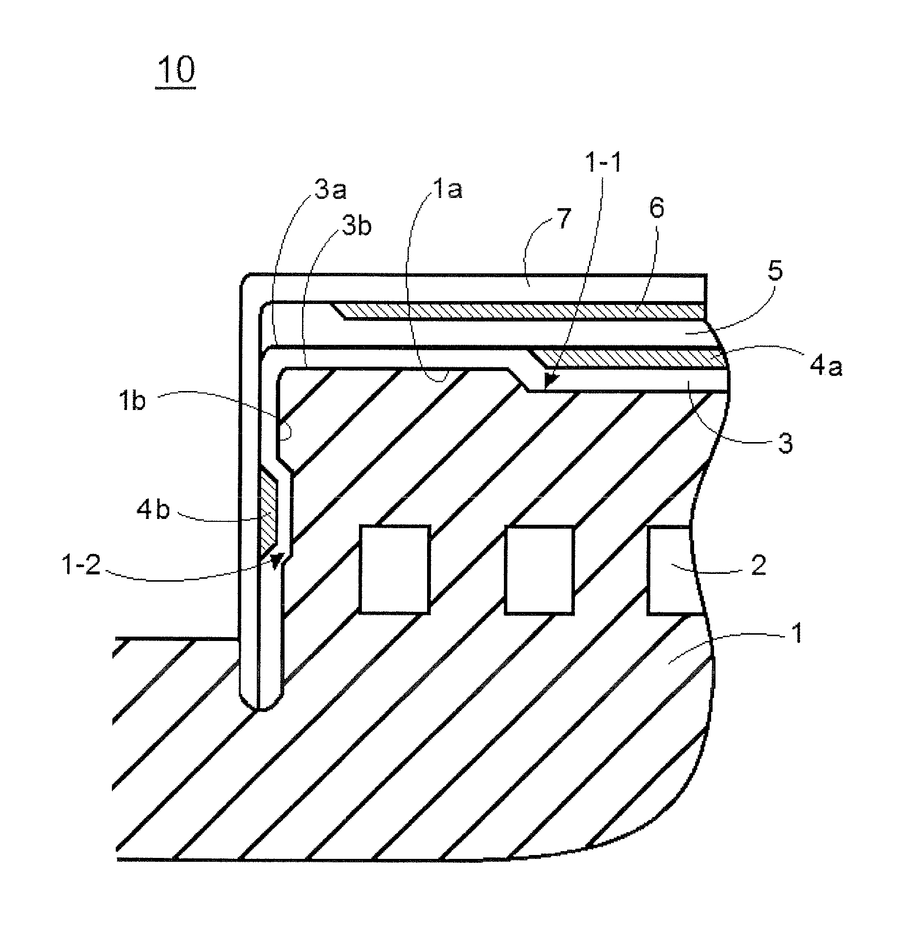
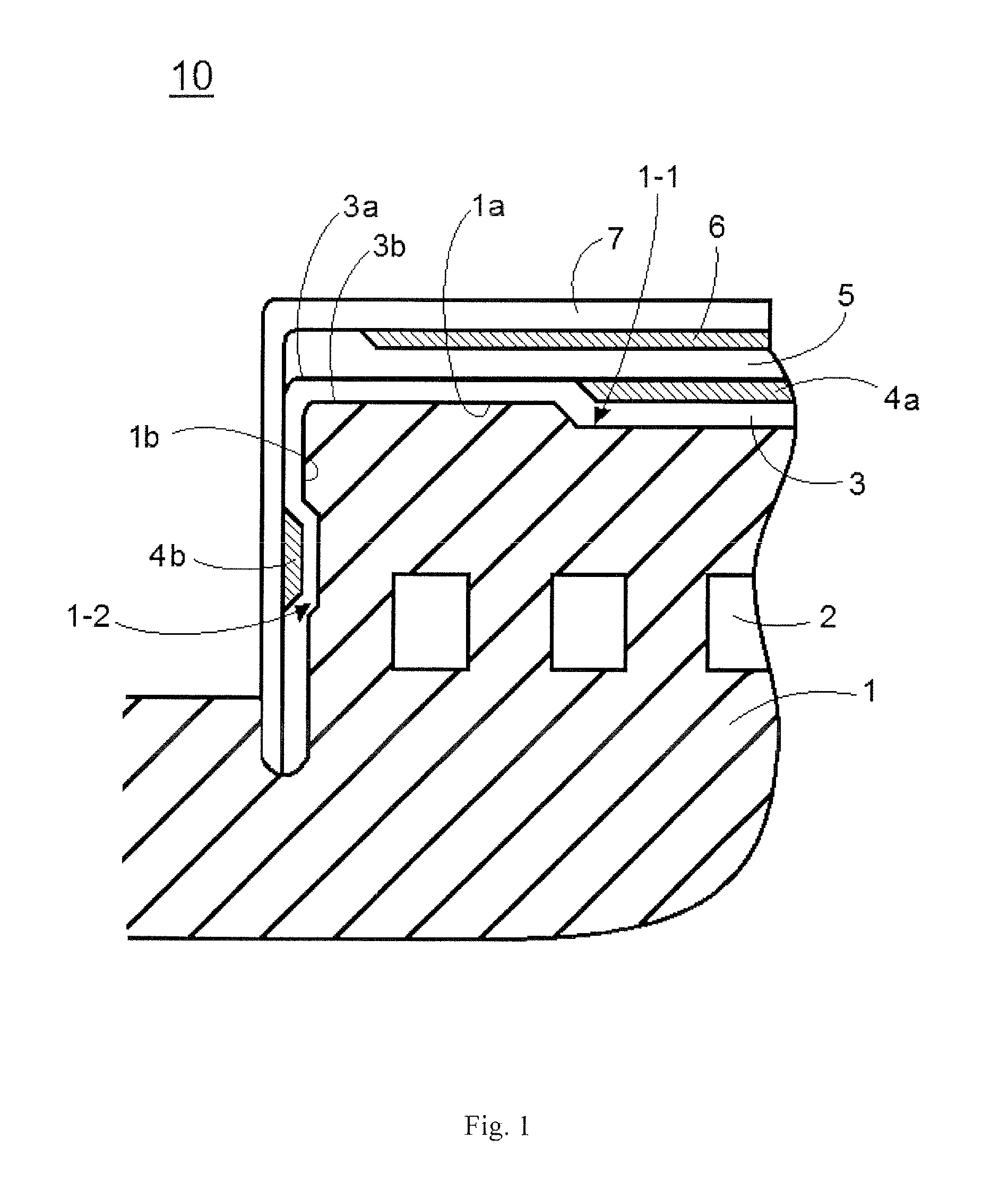
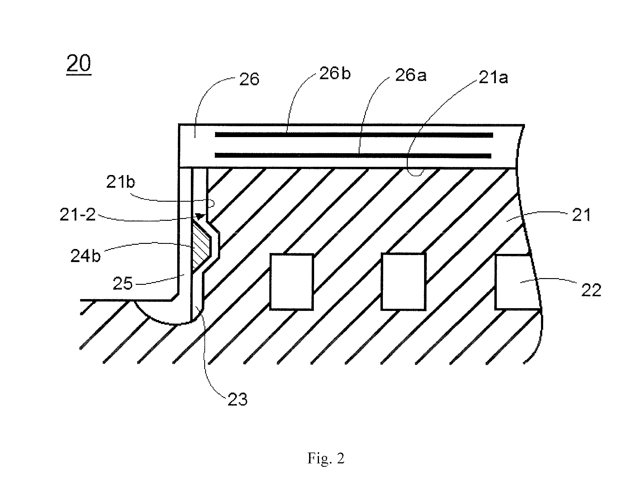
[0063]FIG. 1 is a cross-sectional view of a semiconductor wafer heated electrostatic chuck (ESC) according to one aspect of the present invention. The heated ESC 10 includes a base 1 having cooling channels 2 (i.e., coolant conduits) provided therein when the base is a metal, for example. The base material can be made of a metal, a ceramic or a composite material such as a ceramic material, including, but not limited to aluminum or alumina, for example. Preferably, the coefficient of thermal expansion coefficient (CTE) of the material comprising the base 1 is in a range of 20 to 30 μm / m° C. at 25° C.-227° C., which corresponds to an operating temperature range of the ESC, and is most preferably around 25.2 μm / m° C. This preferred CTE value corresponds to the CTE of a particular aluminum base used by the Applicant, FM Industries. The preferred CTE range is about ±5 μm / m° C. of the CTE of this base material. If the CTE is outside the preferred range, movement due to thermal expansion ...


PUM

PropertyMeasurementUnit
Thicknessaaaaaaaaaa
Porosityaaaaaaaaaa
Coefficient of linear thermal expansionaaaaaaaaaa

Abstract

A heated electrostatic chuck is provided, including a base having an upper surface and peripheral side surfaces, a thermal barrier coating formed by plasma deposition directly on at least the upper surface of the base, at least one heating element formed on portions of the thermal barrier coating, an electrically insulating layer formed on the heating element and exposed portions of the thermal barrier coating, at least one chucking electrode formed on at least a portion of the electrically insulating layer, and a protective layer formed on the chucking electrode.

Description

FIELD OF THE INVENTION[0001]The present invention relates to semiconductor wafer processing apparatus, in particular, electrostatic chucks, semiconductor wafer heaters and heated electrostatic chucks.BACKGROUND OF THE INVENTION[0002]Electrostatic chucks are widely used in the semi-conductor manufacturing industry in order to temporarily hold silicon wafers in place while a variety of manufacturing processes are carried out on the wafers. To this end, such electrostatic chucks include a chucking electrode to create an electrostatic force on the upper surface of the electrostatic chuck.[0003]In order to heat the held wafers during the manufacturing process, electrostatic chucks often include one or more embedded heating elements. In addition, it is very common for the electrostatic chuck to be carried by a metal or ceramic base that includes cooling channels formed therein, with the base acting as a heat sink. Coolant flows through the channels in the base in order to help control a t...

Claims


Application Information

Patent Timeline
IPC IPC(8): H01L21/683
CPCH01L21/6833H01L21/67103Y10T29/49083
Inventor CHO, JAE YONGARGABRIGHT, KEVINLAROCHE, III, JAMES E.NAIM, MAHMOODHAMMERICH, DAVID R.MILLER, JOHN R.
Owner FM INDS
Learn More