Differential Optical Receiver for Avalanche Photodiode and SiPM

a technology of optical receiver and photodiode, applied in the field of light sensors, can solve the problems of limiting the usefulness limiting the performance of high frequency applications, and limiting the use of this prior art,

Active Publication Date: 2014-10-02
EXCELITAS CANADA
View PDF7 Cites 17 Cited by
  • Summary
  • Abstract
  • Description
  • Claims
  • Application Information

AI Technical Summary

Benefits of technology

The present invention provides a differential optical receiver for avalanche photodiode and SiPM. The receiver circuit includes a differential transimpedance amplifier, a photodiode, a high voltage supply source, an impedance element and a high voltage supply variation sensing element. The impedance element is connected to the high voltage supply and the second terminal of the differential transimpedance amplifier. The sensor is connected to the first current mirror and the second input of the differential transimpedance amplifier. The circuit can convert an optical signal into an electrical signal with high efficiency and accuracy.

Problems solved by technology

US Patent application 2004 / 0130397 A1 and U.S. Pat. No. 7,561,812, B2 both target low voltage applications and offer limited performance for high frequency applications using avalanche photodiodes (APD) and not sufficient for a silicon photomultiplier (SiPM).
For high frequency applications using Avalanche Photodiodes or SiPM, a simple capacitance may not accurately model the photodetector and high voltage required to bias the APD or SiPM, limiting the usefulness of this prior art.
Furthermore, both circuits are limited to common mode current (the current injected simultaneously at the inputs of the differential transimpedance amplifier) within the dynamic range of each input of the differential transimpedance amplifier.
This is an important limitation of a system if it is desirable to change the APD gain quickly as it is the case in range finding application where a close target may reflects a significant amount of light back into the receiver thus saturating the receiver and blinding the receiver from detection of targets located in the line of sight at a greater range.
Also, these circuits inject a DC current at the input of the transimpedance amplifier which cannot be used for fast signal variation.

Method used


Image

  • Differential Optical Receiver for Avalanche Photodiode and SiPM
  • Differential Optical Receiver for Avalanche Photodiode and SiPM
  • Differential Optical Receiver for Avalanche Photodiode and SiPM

Examples


first embodiment

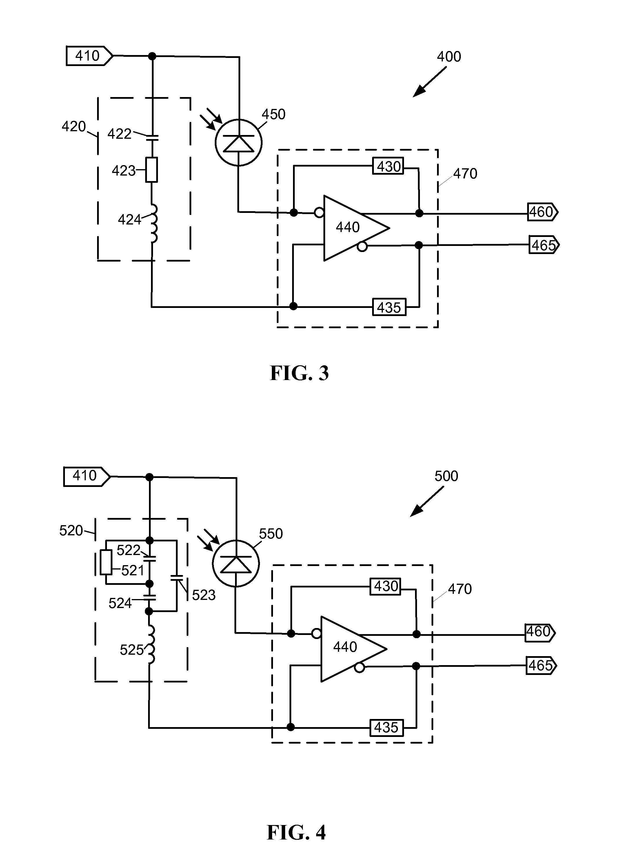
[0031]A first exemplary embodiment of an optical receiver400 is shown in FIG. 3. The first embodiment includes an APD equivalent impedance 420, including a capacitor 422 having equivalent junction capacitance of the APD 450, a resistor 423 with equivalent series resistance of the APD 450 and an inductor 424 with equivalent inductance of the APD 450 interconnected to transimpedance amplifier 470 and the high voltage supply 410. In particular, the APD 450 is disposed between the high voltage supply 410 and a first input of the differential transimpedance amplifier 470, while the APD equivalent impedance 420 is connected between the high voltage supply 410 and a second input to the differential transimpedance amplifier 470 with outputs 460, 465.

exemplary embodiment 500

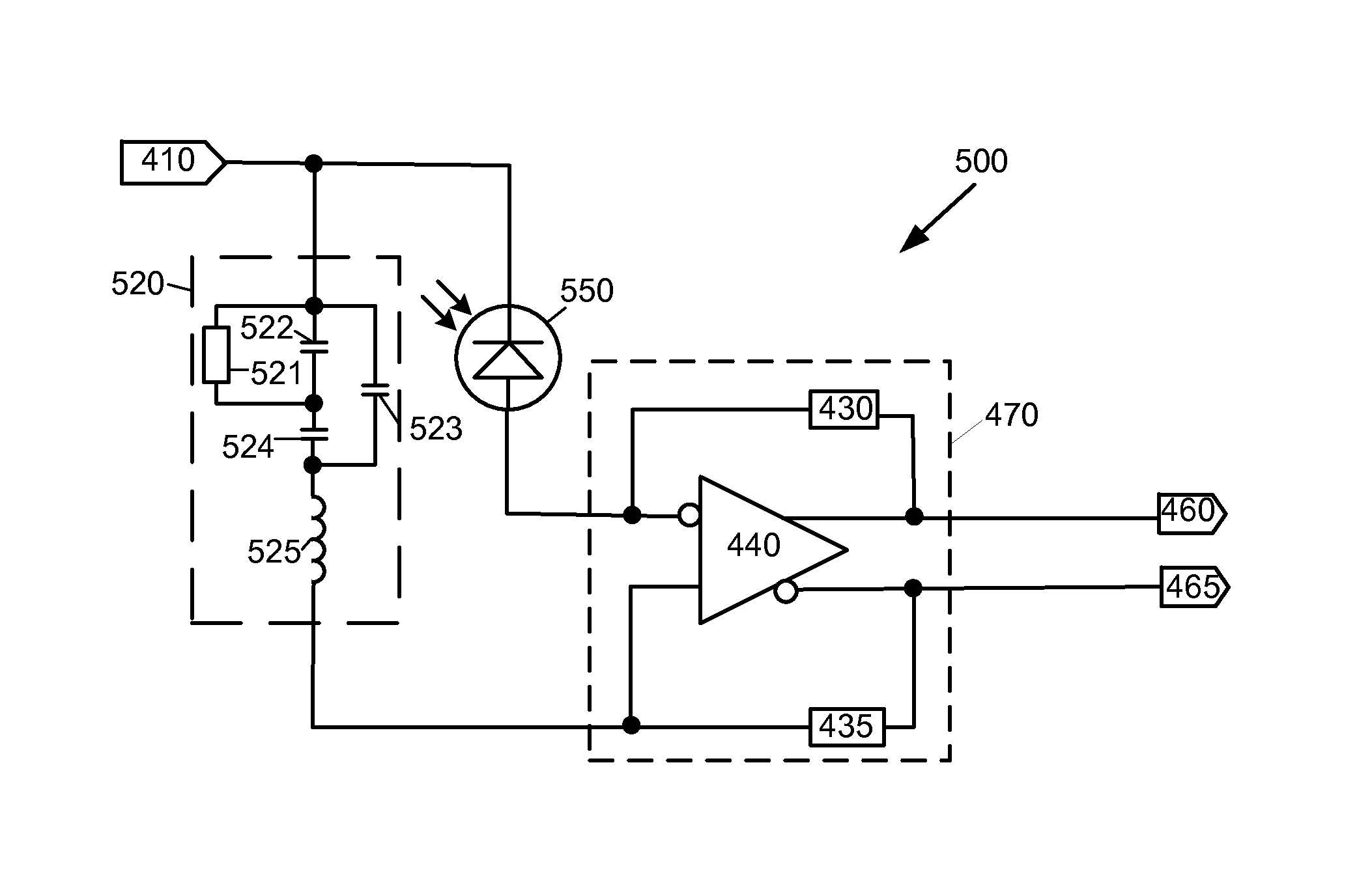
[0032]A second exemplary embodiment 500 is shown in FIG. 4. For a SiPM 550, the voltage sensing element 520 may be built using the equivalent circuit as proposed by Corsi F. et al, “Modeling a silicon photomultiplier (SiPM) as a signal source for optimum front-end design,” Nuclear Instruments and Methods in Physics Research A, 572 (2007), 416-418, where an equivalent SiPM quench resistor 521, a quench capacitor 522, a grid capacitance 523, a junction capacitance 524, and an inductor 525 representing the connection of the SiPM to the transimpedance amplifier 470 are used. The SiPM 550 is disposed between the high voltage supply 410 and the first input of the transimpedance amplifier 470, while the SiPM equivalent impedance 520 is connected between the high voltage supply 410 and the second input to the transimpedance amplifier 470.

[0033]In a third embodiment of an optical receiver 600 shown in FIG. 5, the total output noise of the receiver 600 may be reduced by filtering the second o...

seventh embodiment

[0046]The seventh embodiment optical receiver circuit 1110 configuration, shown by FIG. 9, advantageously uses a differential transimpedance amplifier 1180 where a first input of the differential transimpedance amplifier 1180 is connected to a photodetector 1150 and a second input of the differential transimpedance amplifier 1180 is connected to a high voltage supply 1110 variation sensing element 1122 of equal impedance to the photodetector 1150.

[0047]A second high voltage sensing element 1123 is connected to 2 current mirrors 1191 and 1192 in series which are used to inject a current of equal amplitude at both inputs of the differential transimpedance amplifier 1180.

[0048]Since the input signal of the current mirrors 1191 and 1192 is the same, the current injected in both inputs of the differential transimpedance amplifier 1180, is seen as a common mode signal rejected by the Common Mode Rejection Ratio of the differential transimpedance amplifier 1180.

[0049]The two current mirror...


PUM


Abstract

A device and method to immune an APD or SiPM optical receiver against photodetector voltage supply variation is presented. A differential trans-impedance amplifier includes one input connected to the photodetector and the other input connected to a high voltage supply variation sensing device. The sensing element includes a circuit replicating the impedance of the photodetector.

Description

FIELD OF THE INVENTION[0001]The present invention relates to light sensors, and more particularly, is related to a photodetector circuit.BACKGROUND OF THE INVENTION[0002]Photodetectors are used to detect light of a given wavelength and produce a current proportional to the intensity of the detected light. A photodetector may be supplied with a bias voltage. The output of the photodetector may vary with variations of the bias voltage.[0003]A prior art photodetector circuit 100 is shown in FIG. 1. The circuit includes a photodetector 150 between a high voltage supply 110 and a transimpedance amplifier 170 (TIA) including a voltage amplifier 140 and a feedback resistor 130. The signal (photocurrent) from the photodetector 150 is amplified by the transimpedance amplifier 170, thereby converting a photocurrent from the detector into a voltage 160 suitable for post processing, for example, by a post processing circuit (not shown).[0004]Any variation of the high voltage supply 110 is coupl...

Claims


Application Information

Patent Timeline
IPC IPC(8): H01L31/02
CPCH01L31/02H03F3/087H01L31/02027H01L31/02016
Inventor LAFORCE, FREDERIC
Owner EXCELITAS CANADA
Why Eureka
Try Eureka