Electron emission element and method for manufacturing the same

a technology of electron emission element and manufacturing method, which is applied in the manufacture of electrode systems, electric discharge tubes/lamps, superimposed coating processes, etc., can solve the problems of large power consumption, difficult to form x-ray tubes in a small size, and high production cost, so as to reduce the damage of a structural aspect ratio of carbon nano tubes, the work function of electron emission devices, and the effect of reducing the damag

Inactive Publication Date: 2014-10-02
INTELLECTUAL DISCOVERY CO LTD
View PDF0 Cites 13 Cited by
  • Summary
  • Abstract
  • Description
  • Claims
  • Application Information

AI Technical Summary

Benefits of technology

[0013]By coating lithium at a carbon nano tube, a work function of an electron emission device is lowered and thus an electric field turn-on electric field can be reduced. As a result, an emission current greatly increases and thus damage of a structural aspect ratio of a carbon nano tube can be reduced. Further, because a lithium layer protects a surface of the carbon nano tube upon electric field emission, even when the carbon nano tube is used for a long time, a surface thereof can be prevented from being damaged. As a result, because a cold cathode for a ultra-small high resolution X-ray system can be produced, a low turn-on voltage, a high emission current, and stability for a long time can be secured.

Problems solved by technology

Conventionally, an X-ray tube using a thermal electron emission source such as a tungsten filament has been widely used, but a much production cost is required, operation is performed in a high temperature condition, and power consumption is large.
Particularly, because upon applying as a micro focusing X-ray electron source, it is difficult to form the X-ray tube in a small size and the X-ray tube is less used due to a short life-span.
In such a structure, because of multi-layered structural characteristics, the structure has large contact resistance, thereby the large contact resistance becomes a cause that reduces a voltage supply for electron emission and therefore when the X-ray tube operates in a high pressure for a long time, a much heat occurs and adhesion is thus deteriorated.
Therefore, important characteristics of a threshold voltage, a maximum emission current, reliability, and a life-span are deteriorated.

Method used


Image

  • Electron emission element and method for manufacturing the same
  • Electron emission element and method for manufacturing the same
  • Electron emission element and method for manufacturing the same

Examples


experimental example

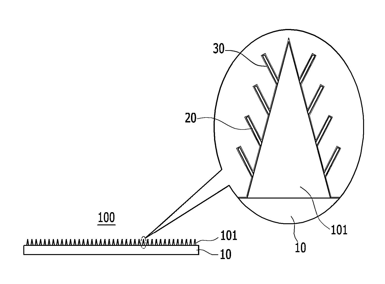
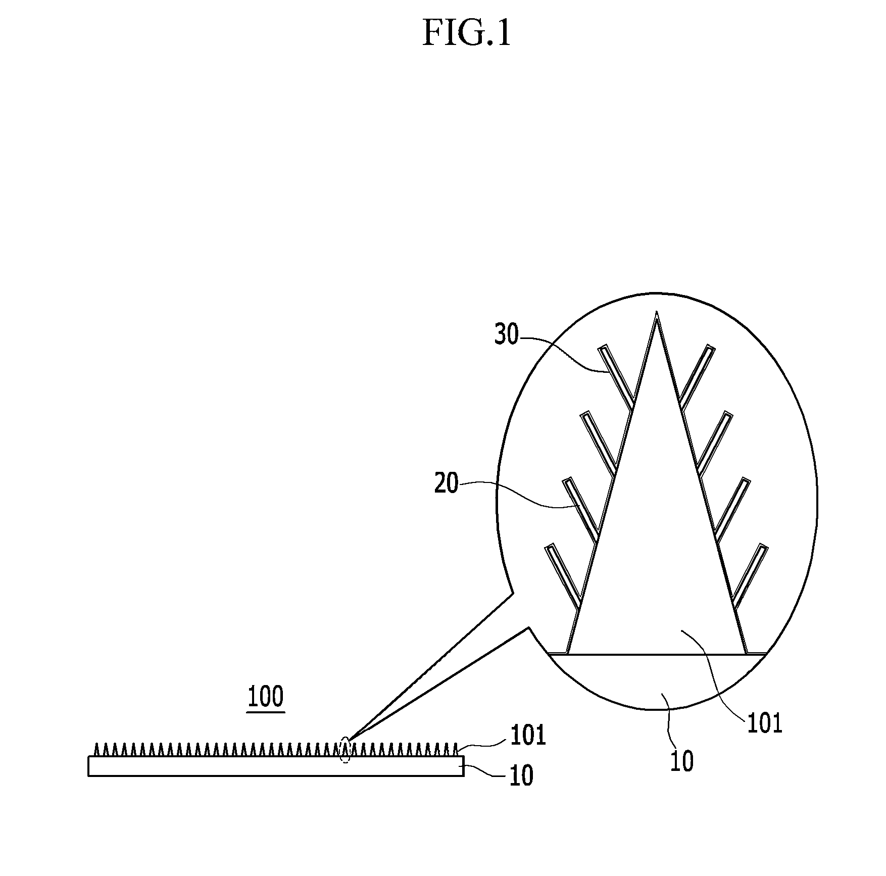
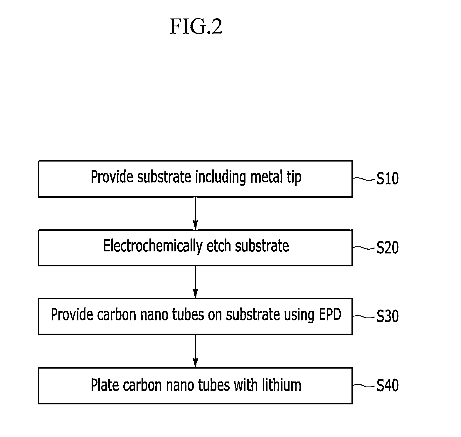
[0051]A substrate having a cone type tip that is formed with a tungsten wire having a diameter of 300 μm was produced. By electrochemically etching the substrate in a solution of KOH of 2 mol, a diameter of the cone type tip was adjusted to about 500 nm. Next, multi-layered wall carbon nano tubes having a diameter of 3 nm to 9 nm were deposited at the substrate using EPD. After carbon nano tube powder of 10 mg was washed with a ratio of one-to-one in a mixed solution of HNO3 and H2SO4 for 5 hours, by injecting the carbon nano tube powder into a mixed solution of isopropyl alcohol of 50 ml and Mg(NO3)26H2O of 15 mg, a suspension was produced. After positioning the substrate as a negative electrode and positioning silicon as a positive electrode at the produced suspension, the carbon nano tubes were deposited on the tip with a DC voltage of 80V for 40 seconds. Here, a distance between the positive electrode and the negative electrode was fixed to 10 mm.

[0052]In a solution including et...

experimental example 1

[0054]By applying a DC voltage of 4V for 1 second, a lithium thin film was coated on carbon nano tubes.

experimental example 2

[0055]By applying a DC voltage of 4V for 2 seconds, a lithium thin film was coated on carbon nano tubes.


PUM

PropertyMeasurementUnit
thicknessaaaaaaaaaa
thicknessaaaaaaaaaa
diameteraaaaaaaaaa

Abstract

An electron emission device and a method of manufacturing the same are provided. The electron emission device includes: i) a substrate including a metal tip; ii) carbon nano tubes that are positioned on the metal tip; and iii) a lithium layer that is positioned on the carbon nano tubes.

Description

CROSS-REFERENCE TO RELATED APPLICATION[0001]This application is related to Korean Patent Application No. 2013-0033107 that was filed in the Korean Industrial Property Office on Mar. 27, 2013, “Enhancement of electron-emission and long-term stability in tip-type carbon nanotube field emitters by lithium coating”, which is a material that was announced at the 39th ICMC on Apr. 23, 2012, and “Enhancement of electron emission and long-term stability of tip-type carbon nanotube field emitters via lithium coating”, which is a thesis that was issued on Nov. 6, 2012.BACKGROUND OF THE INVENTION[0002](a) Field of the Invention[0003]The present invention relates to an electron emission device and a method of manufacturing the same. More particularly, the present invention relates to an electron emission device and a method of manufacturing the same that embody a high current density and a high electron emission degree by coating lithium.[0004](b) Description of the Related Art[0005]Due to exce...

Claims


Application Information

Patent Timeline
Patent Type & Authority Applications(United States)
IPC IPC(8): H01J1/304H01J9/00
CPCH01J1/3044H01J9/00Y10S977/842Y10S977/939B82Y40/00B82Y30/00H01J9/025H01J2201/30411H01J2201/30434H01J1/304H01J9/02
Inventor PARK, JIN SEOKKIM, BU JONGKIM, WONLEE, SANG HYUK
Owner INTELLECTUAL DISCOVERY CO LTD
Why Eureka
Try Eureka