Semiconductor light-emitting device

a semiconductor and light-emitting device technology, applied in the direction of semiconductor devices, basic electric elements, electrical equipment, etc., can solve the problems of increased device forward voltage, strong band structure distortion, and inevitable generation of interface space charges, so as to mitigate the band edge tilt, reduce the effect of polarization field induced band structure distortion

Inactive Publication Date: 2014-11-13
QINGDAO JASON ELECTRIC
View PDF2 Cites 18 Cited by
  • Summary
  • Abstract
  • Description
  • Claims
  • Application Information

AI Technical Summary

Benefits of technology

[0009]According to one aspect of the present invention, composition grading, for example, Al-composition grading is used to modify the band structure of polar semiconductor heterostructures in order to mitigate the polarization field induced band structure distortion. Al-composition changes can result in AlInGaN bandgap width changes. For example, increasing Al-composition can enlarge the bandgap width, enabling conduction band moving upwards and valence band moving downwards. These movements can be used to mitigate the band edge tilt arising from the polarization field of polar semiconductor heterostructures. In some embodiments, composition grading is used to alleviate the band edge tilt in quantum wells and quantum barriers, leading to improved device forward voltage and quantum efficiency.

Problems solved by technology

This means that interface space charges are inevitably generated when forming heterostructures using nitrides, due to the discontinuity of spontaneous and piezoelectric polarizations at the heterointerface.
The spontaneous and piezoelectric polarizations in nitrides have maximal values along c-direction (), and the resultant interface space charge density in GaN / InGaN and AlGaN / AlGaN c-oriented heterostructures can exceed 1013 / cm2, leading to electric field larger than 1 MV / cm resulting in strong band structure distortion.
These effects lead to higher device forward voltage and lower internal quantum efficiency, respectively.
However, since the optimal incorporation conditions of Al and In are not compatible with each other, it is difficult to obtain high-quality AlInGaN quaternary materials.

Method used


Image

  • Semiconductor light-emitting device
  • Semiconductor light-emitting device
  • Semiconductor light-emitting device

Examples


embodiment 1

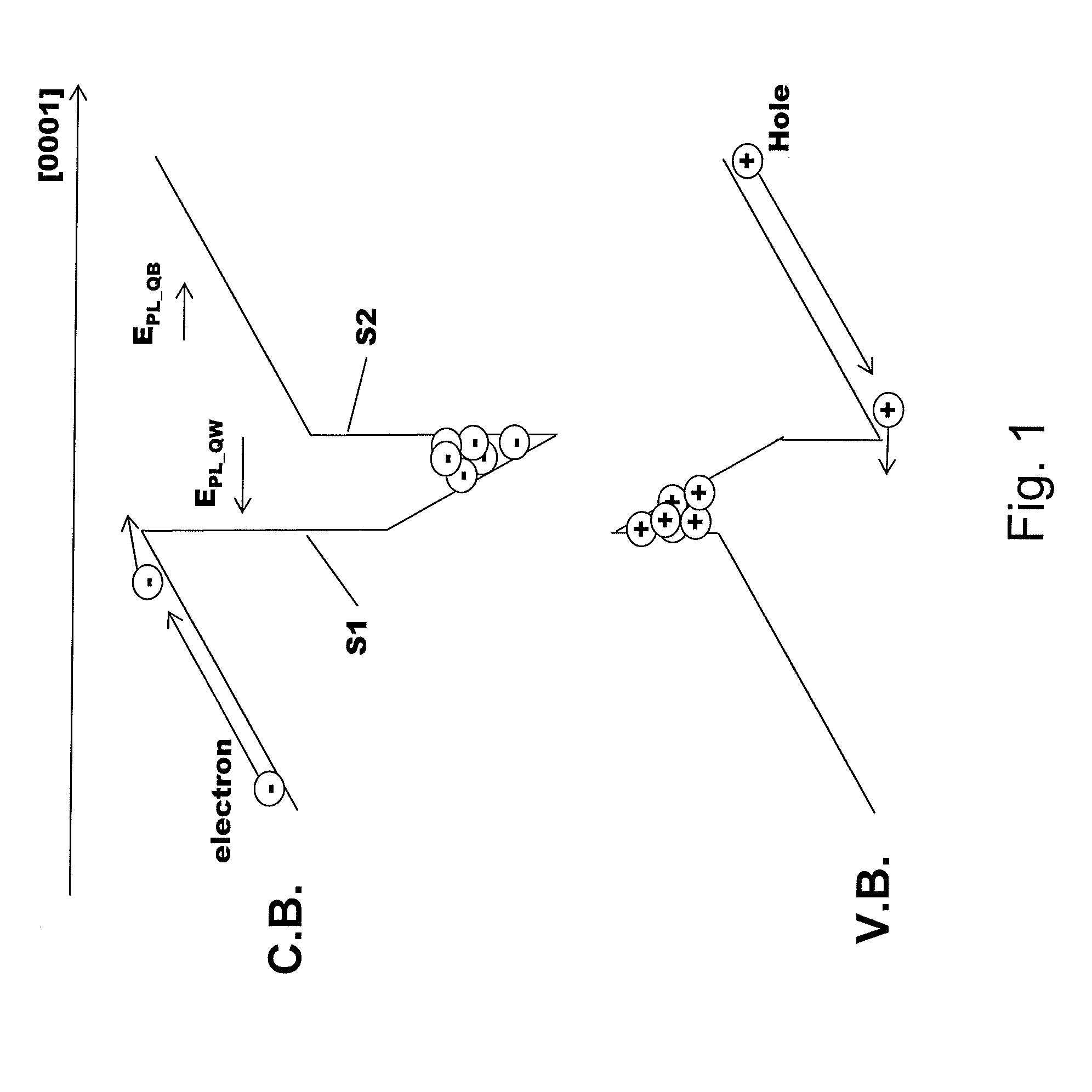
[0031 according to the present invention is a wurtzite [0001]-oriented group III nitride ultraviolet light emitting diode, with the layered structure illustrated in FIG. 4. As shown substrate 10 can be selected from (111) Si, (0001) sapphire (flat or patterned), AlN, GaN, AlGaN, and the like. Formed over substrate 10 is layer 20 as epitaxy template, preferably being made of AlN, or AlGaN with high Al-composition (e.g. higher than 60%). The thickness of layer 20 is preferably to be more than 100 nm, for example, 1000-3000 nm. Following layer 20 is layer 40 serving as electron supplier layer made of N-type AlGaN, with enough thickness for good electrical conduction and material quality, preferably to be 2 μm or thicker. In order to improve the material quality of layer 40, optionally inserted in-between layer 20 and layer 40 is a strain management and defect filtering structure 30. Structure 30 can be AlGaN / AlGaN multiple-layer heterostructure, or AlN / AlGaN multiple-layer heterostruct...

embodiment 4

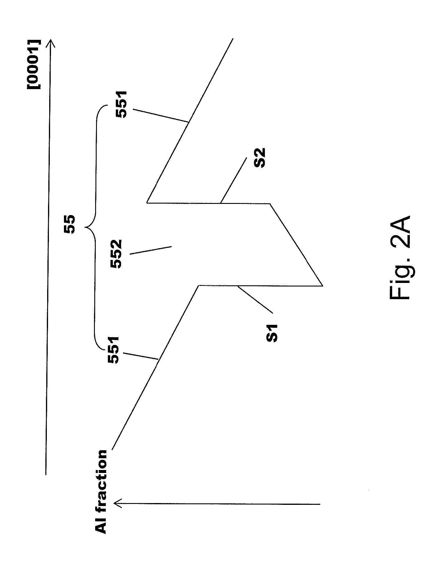
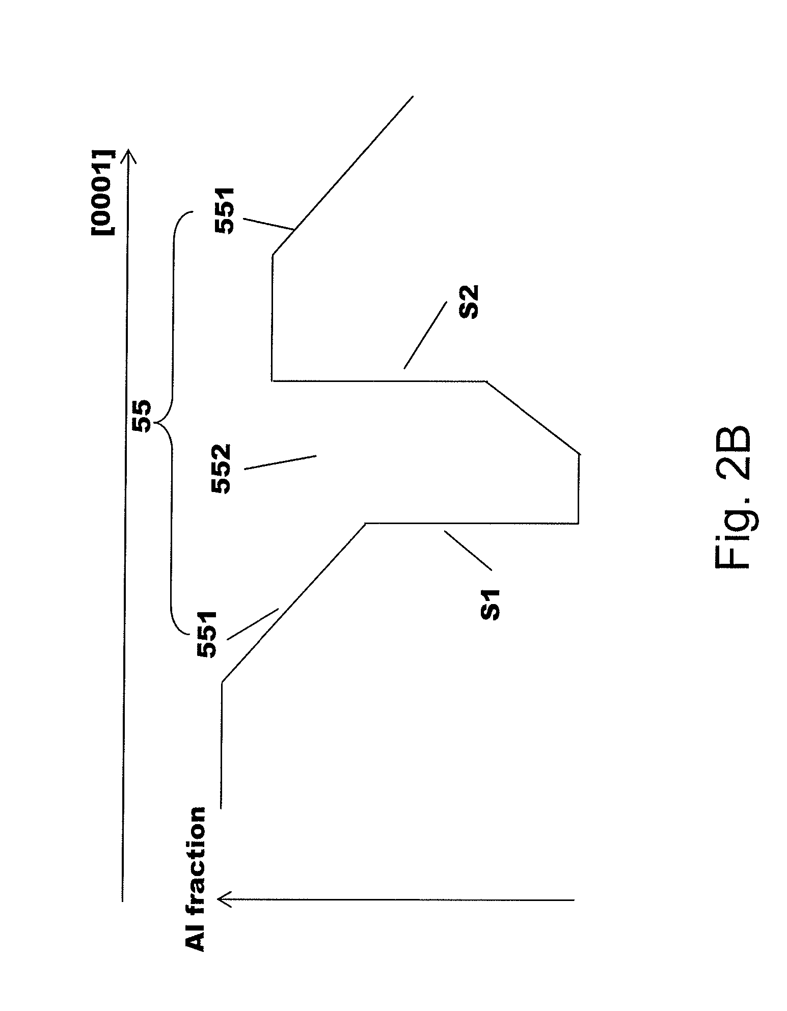
[0047 distinguishes from embodiment 1 in terms of the MQW active-region doping. For this embodiment, the Al-composition and donor concentration ([D]) distributions in one quantum well and two quantum barriers of the MQW active-region 55 are illustrated in FIG. 2C. As seen, besides the Al-composition grading within the MQW, donor concentration within the MQW is also graded. Along the epitaxy direction ([0001]), donor concentration [D] in the quantum barriers increases, while [D] in the quantum wells can be zero or a constant value, or preferably gradually decrease. Preferably, as illustrated in FIG. 2C, the donor concentration in the quantum wells and quantum barriers possess gradual linear changes. It can also have gradual nonlinear changes and abrupt changes such as stair-case changes.

[0048]The donor can be Si or Ge. In quantum barriers 551 the donor concentration can increase from zero to 1×1019 cm −3, or from 1×1017 cm−3 to 1×1019 cm −3,along the epitaxy direction [0001]. When po...


PUM


Abstract

The present invention presents a solid-state semiconductor light emitting device with reduced forward voltage and improved quantum efficiency. The light emitting device is characterized by its multiple-quantum-well active-region with opposite composition grading in the quantum barriers and quantum wells along the device epitaxy direction.

Description

CROSS-REFERENCE TO RELATED APPLICATION[0001]This application claims priority benefit of Chinese patent application serial No. 201310168615.0 filed on May 9, 2013. The entirety of the above-mentioned patent application is hereby incorporated by reference herein and made a part of this specification.FIELD OF THE INVENTION [0002]The present invention relates in general to light-emitting device made of polar semiconductors, more particularly to light-emitting device made of group III nitride polar semiconductors with composition gradient in the active-region.DESCRIPTION OF THE RELATED ART [0003]Nitride based light-emitting diodes (LEDs) have achieved fast progress in recent years. In the visible spectrum regime, InGaN LEDs are increasingly challenging traditional lighting sources such as fluorescent lamps, due to their technological and economical advantages. Currently, high-efficiency InGaN LED white light lamps with efficacy over 130 lm / watt are commercially available. In the ultravio...

Claims


Application Information

Patent Timeline
Patent Type & Authority Applications(United States)
IPC IPC(8): H01L33/06
CPCH01L33/06H01L33/0025H01L33/32
Inventor ZHANG, JIANPING
Owner QINGDAO JASON ELECTRIC
Why Eureka
Try Eureka