Enhanced Performance Active Pixel Array and Epitaxial Growth Method for Achieving the Same

Active Publication Date: 2014-11-27
OSTENDO TECH INC
View PDF3 Cites 16 Cited by
  • Summary
  • Abstract
  • Description
  • Claims
  • Application Information

AI Technical Summary

Problems solved by technology

However, such lighting applications depend on high luminous flux emanating from the imager's pixel array.
Inefficient light emitters convert electric current to heat via non-radiative recombination, which further degrades emitter efficiency and risks thermal damage to the light emitter and/or thermally coupled electronics and optics.
A significant drawback to such heteroepitaxy, however, is the tendency for elevated densities of threading dislocations to form.
III-nitride semiconductor light emitters have historically been grown heteroepitaxially due to the limited availability of native GaN, AIN, or InN substrates.
Such high dislocation densities dramatically reduce the radiative recombination efficiency of III-nitride light emitters and increase heat generation, making such light emitters less desirable for illumination and display applications.
While much progress has been made in the development of pola

Method used


Image

  • Enhanced Performance Active Pixel Array and Epitaxial Growth Method for Achieving the Same
  • Enhanced Performance Active Pixel Array and Epitaxial Growth Method for Achieving the Same
  • Enhanced Performance Active Pixel Array and Epitaxial Growth Method for Achieving the Same

Examples


Embodiment Construction

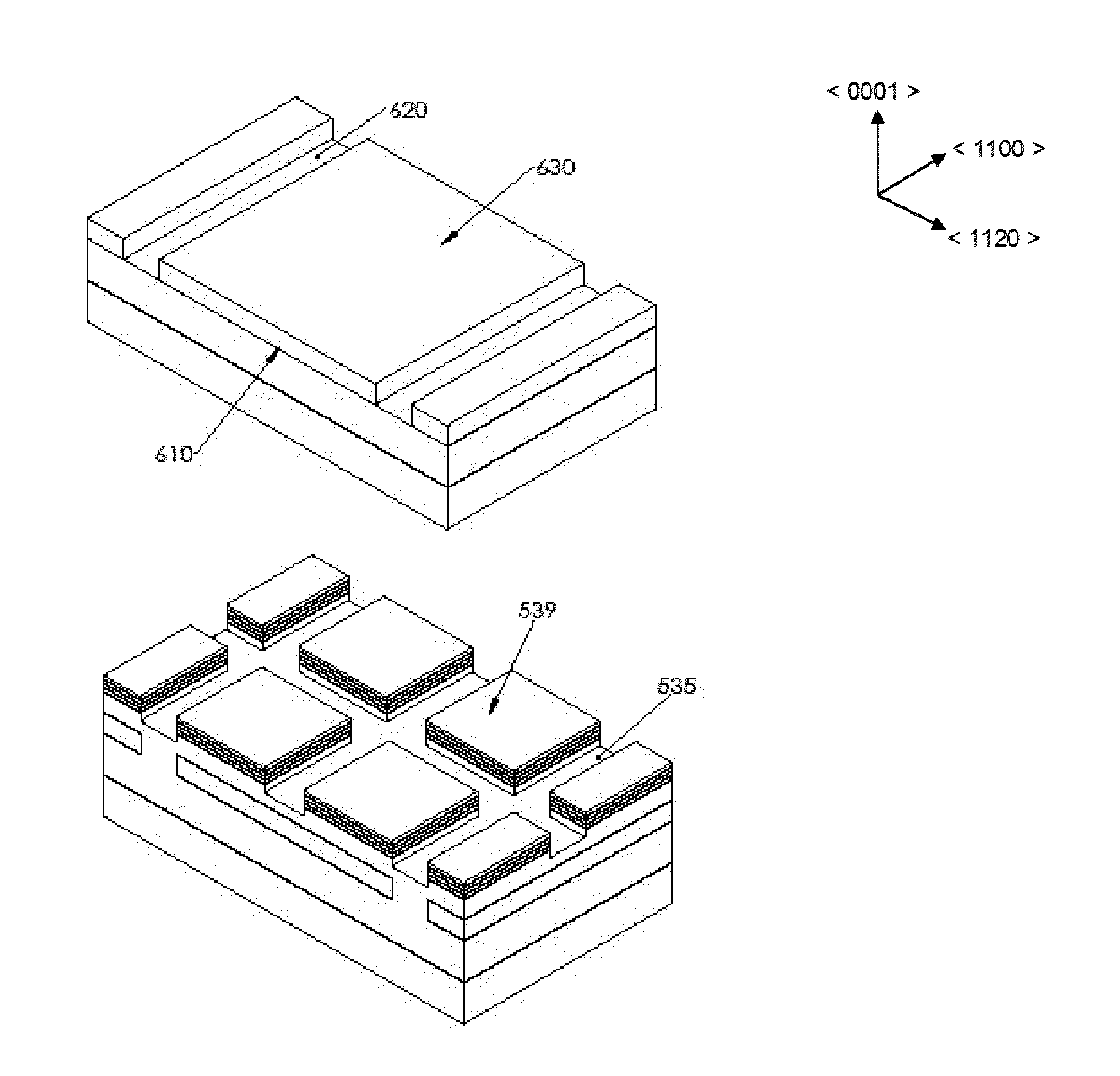
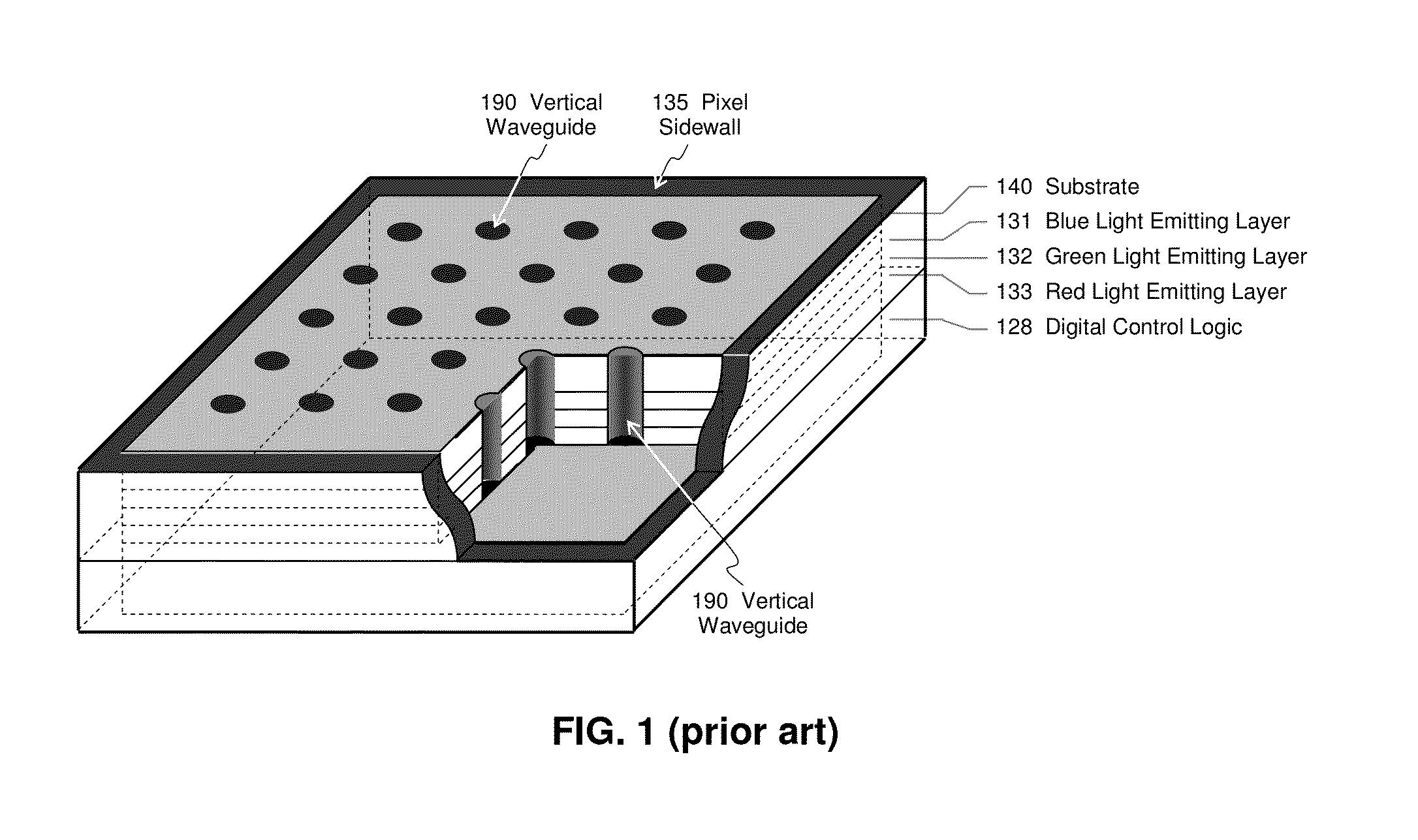
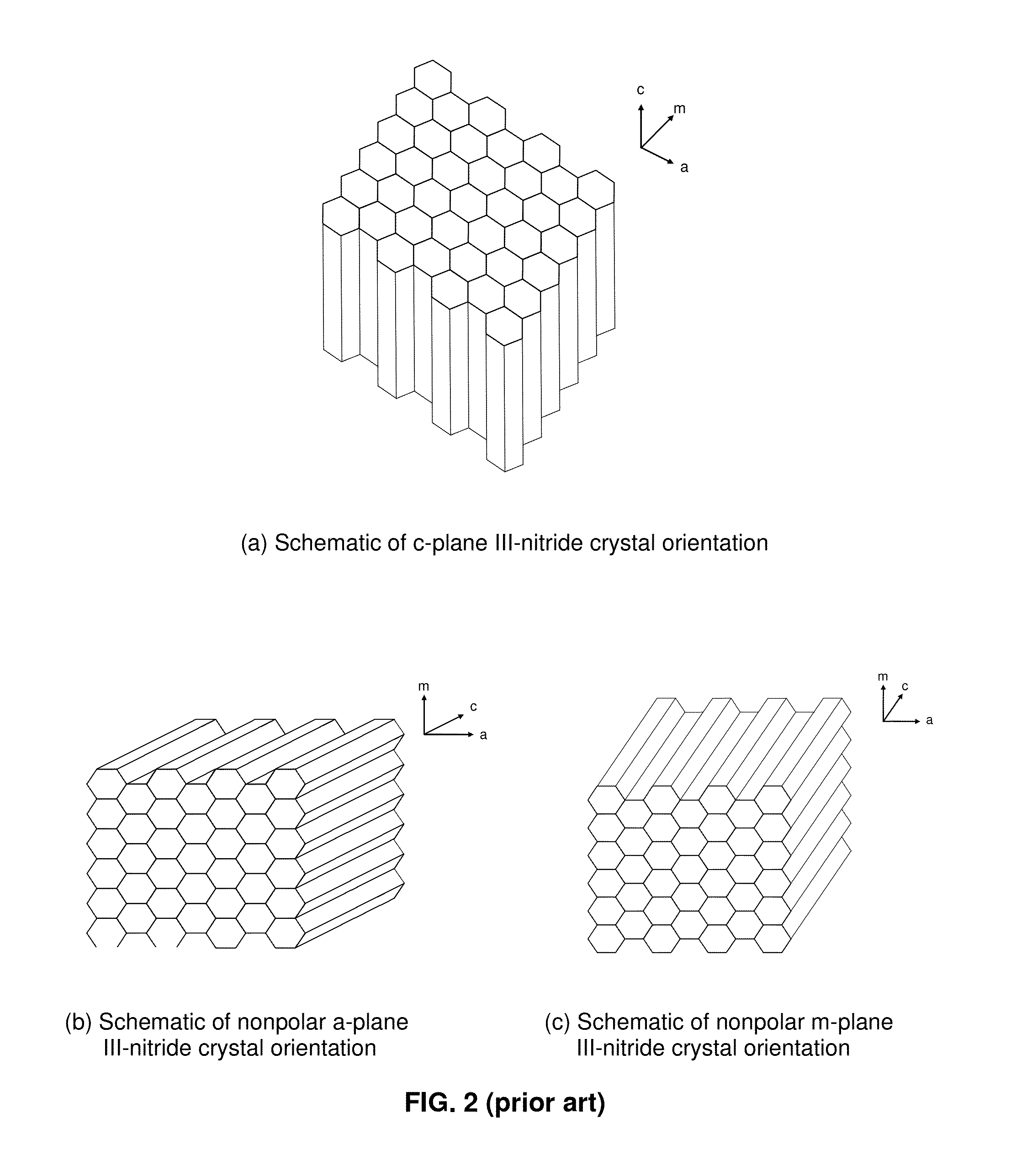
[0058]A new class of emissive micro-scale pixel array devices has been recently introduced Ref [1-6]. These devices are solid state light (SSL) based and feature high brightness, very fast light multi-color intensity and spatial modulation capabilities in a very small single device size that includes all the drive circuitry. The SSL light emitting pixels of one such a device may be either a light emitting diode (LED) or laser diode (LD) whose on-off state is controlled by the drive circuitry contained within a CMOS chip (or device) upon which the emissive micro-scale pixel array is bonded. The size of the pixels comprising the emissive array of such devices would typically be in the range of approximately 5-20 micron with the typical emissive surface area of the device being in the range of approximately 15-150 square millimeter. The pixels within the emissive micro-scale pixel array device are individually addressable spatially, chromatically and temporally, typically through the d...


PUM


Abstract

Methods are described to utilize relatively low cost substrates and processing methods to achieve enhanced emissive imager pixel performance via selective epitaxial growth. An emissive imaging array is coupled with one or more patterned compound semiconductor light emitting structures grown on a second patterned and selectively grown compound semiconductor template article. The proper design and execution of the patterning and epitaxial growth steps, coupled with alignment of the epitaxial structures with the imaging array, results in enhanced performance of the emissive imager. The increased luminous flux achieved enables use of such images for high brightness display and illumination applications.

Description

CROSS-REFERENCE TO RELATED APPLICATIONS[0001]This application is a continuation of International Application No. PCT / US2014 / 029627 filed Mar. 14, 2014 which claims the benefit of U.S. Provisional Patent Application No. 61 / 800,076 filed Mar. 15, 2013.BACKGROUND OF THE INVENTION[0002]1. Field of the Invention[0003]The present invention relates to emissive imager devices comprising monolithic semiconductor arrays of multicolor light emitters that can be used as an image or light sources for display, projection or illumination applications. The invention further relates to epitaxial growth of compound semiconductor layers for use in the emissive imager, and methods to improve the quality and performance thereof. The invention further relates to the epitaxial growth of compound semiconductor template layers having periodic arrays of reduced defect density suitable for production of superior performance light emitting devices.[0004]2. Prior ArtREFERENCES CITED[0005][1] U.S. Pat. No. 7,623...

Claims


Application Information

Patent Timeline
IPC IPC(8): H01L33/00H01S5/026H01S5/30
CPCH01L33/0062H01L33/0066H01L33/0075H01L2933/0025H01S5/3013H01S5/026H01L33/007H01L21/0242H01L21/02538H01L21/0254H01L21/02642H01L21/02647H01L27/156H01L33/08H01L33/16
Inventor EL-GHOROURY, HUSSEIN S.HASKELL, BENJAMIN A.
Owner OSTENDO TECH INC
Why Eureka
Try Eureka