Method For Filling Recesses Using Pre-Treatment With Hydrocarbon-Containing Gas

a hydrocarbon-containing gas and recess technology, applied in the direction of coatings, metallic material coating processes, chemical vapor deposition coatings, etc., can solve the problems of copper losing its advantage, increasing resistivity, and affecting the signal delay and power consumption. high

Active Publication Date: 2014-12-11
ASM IP HLDG BV
View PDF2 Cites 333 Cited by
  • Summary
  • Abstract
  • Description
  • Claims
  • Application Information

AI Technical Summary

Benefits of technology

[0011]In some embodiments of the present invention, provided is flowable CVD technology to fill recesses of a substrate with flowable film at a high flatness even when line spaces are small or regardless of the line spaces, and even when the recesses are shallow. Some embodiments provides a pre-deposition step performed, prior to a deposition step, to subject surfaces of recesses of a substrate to hydrophobic treatment using a pre-deposition gas or precursor which may be a hydrocarbon gas or a gas having at least one hydrocarbon unit in its molecule, such as a silazane compound having at least one hydrocarbon unit. The surfaces of the recesses to be treated include top surfaces, side walls, and bottom surfaces of the recesses, and top and side surfaces of wiring parts placed at bottoms of the recesses. The pre-deposition gas can become reactive or excited by applying any suitable energy such as heat, UV light, IR light, or plasma to the gas, or if the pre-deposition gas is highly reactive with terminal groups on a surface, the pre-deposition gas can become reactive simply by flowing over the surface under a vacuum. In some embodiments, the pre-deposition step can be conducted in-situ, i,e., in a reactor, immediately followed by a deposition step in the same reactor. In some embodiments, the hydrophobicity of the treated surfaces are such that the water contact angle of the treated surfaces at room temperature can increase to more than about 80°, for example. In some embodiments, by the pre-deposition step, a flatness (a ratio of the lowest thickness in a recess to the height of the recess) of the resultant surface of the substrate after filling the recesses can be improved from about 20% (without the pre-deposition step) to about 75%, for example. Further, in some embodiments, the pre-deposition step can be applied to any suitable flowable film, regardless of the type of flowable film. Also, in some embodiments, the pre-deposition step does not affect the properties of a resultant insulation film converted from a flowable film. As described above, the pre-deposition step can bring about the surprising effects and is a highly effective method to form flattened surfaces of filled recesses.

Problems solved by technology

As micro-fabrication of wiring progresses, signal delay and increase of power consumption becomes problematic due to the increase of line capacity of wiring in the multilayer wiring structure.
However, if micro-fabrication of wiring continues, copper used as a wiring material will increase its resistivity due to the width of wiring being too narrow, and as a result, copper loses its advantage.
Since copper diffuses easily in a low-k film, if it is used as wiring material, it is required that additional complicated steps such as those for stopping the diffusion be taken.
However, with conventional CVD methods, as the space between wires is extremely narrow, the space is difficult to be filled with a low-k film, and voids and the like are formed in the low-k film.
Because of this unevenness, there is a challenge in filling all places until all grooves are filled so as to provide a flat surface by a flowable CVD method.
Also, if the film is too thick, a problem such as film-cracking occurs.
However, with this method, a catalyst itself cannot evaporate and is left in a material, and therefore, this flowable CVD film-forming method does not significantly improve the filling properties.
However, with this method, there are problems such as generation of voids formed in the film after the film-forming process, and an extremely large amount of silanol contained in the material causing corrosion of metal and causing imperfect wiring.
As a general pre-treatment, a plasma treatment using a plasma of an inactive gas such as He and Ar, and a reduction treatment using a hydrogen plasma are known, but those methods have not improved the flatness of the film surfaces.

Method used


Image

  • Method For Filling Recesses Using Pre-Treatment With Hydrocarbon-Containing Gas
  • Method For Filling Recesses Using Pre-Treatment With Hydrocarbon-Containing Gas
  • Method For Filling Recesses Using Pre-Treatment With Hydrocarbon-Containing Gas

Examples


example 1

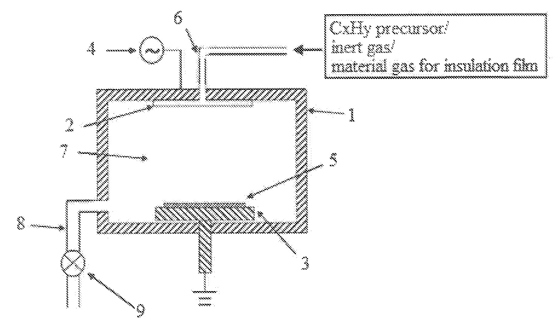
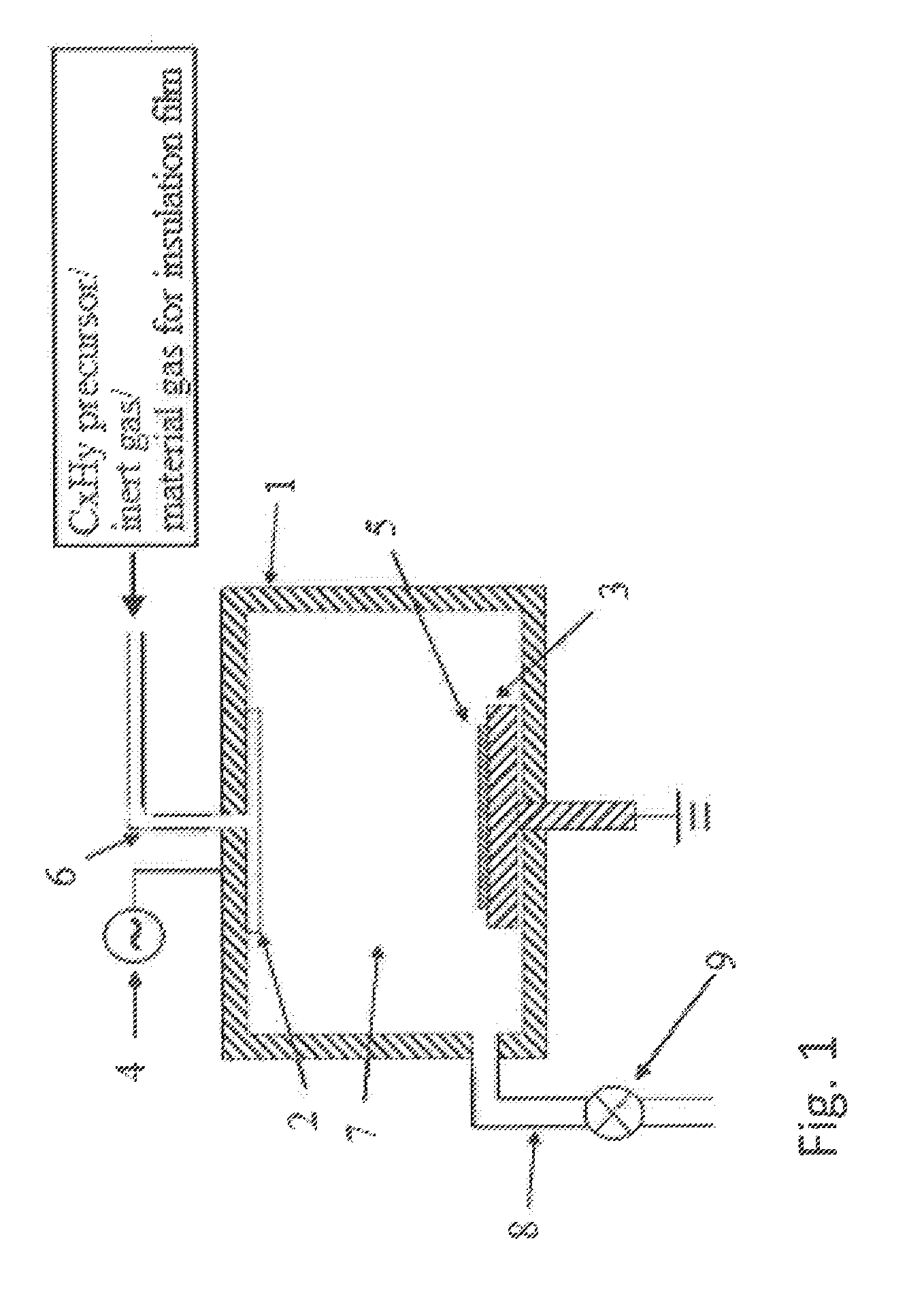
[0052]The pre-deposition step was conducted under the following conditions:

TABLE 3Substrate temperature20°C.Pressure700PaGas used for pre-deposition stephexane (234 sccm)RF power200WDistance between electrodes9mmDuration60seconds

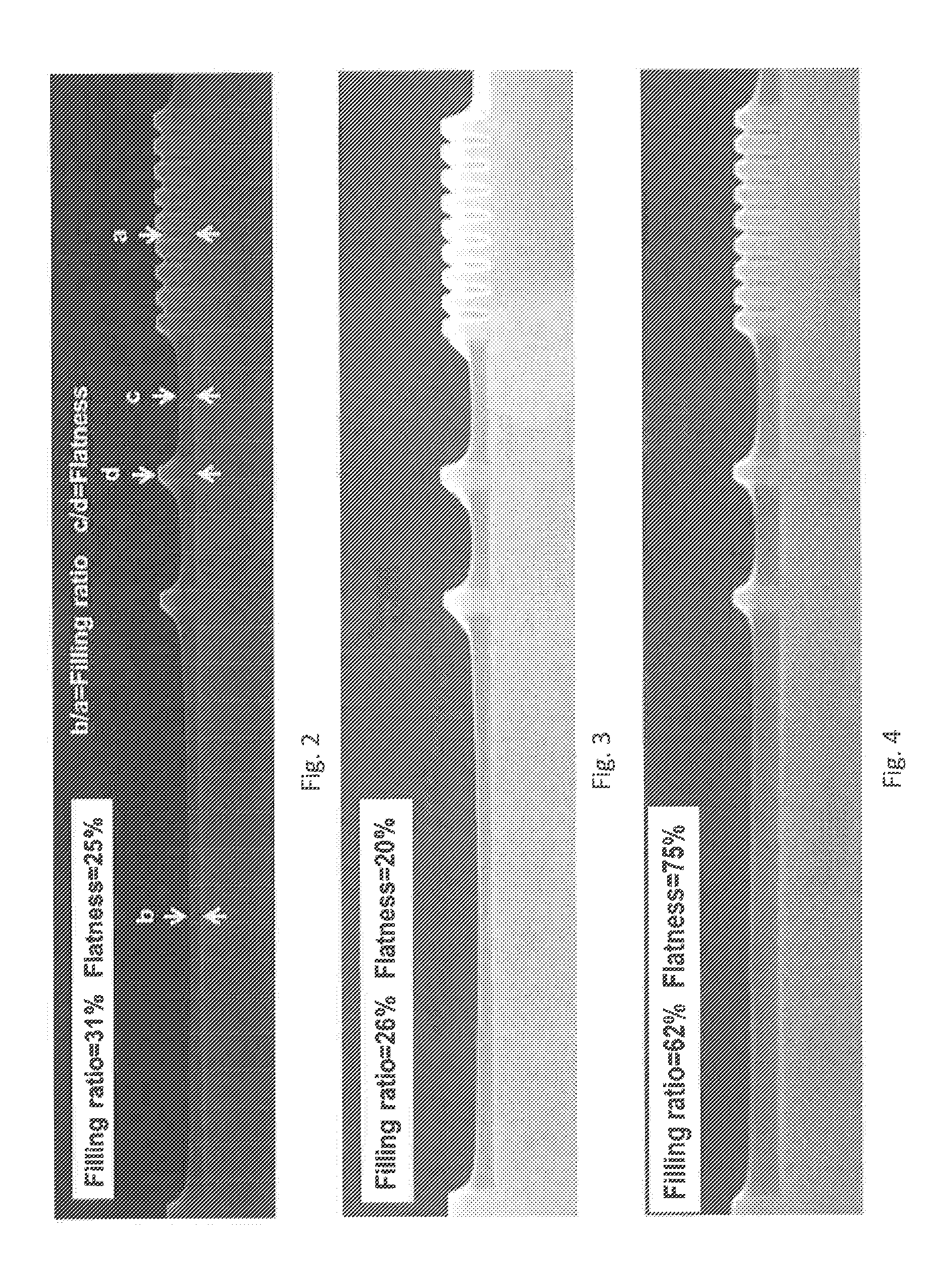
[0053]The deposition step was continuously conducted after the pre-deposition step to deposit a low-k film. As a result, the recesses were filled with the low-k film as shown in FIG. 4, and the filling ratio and the flatness were measured. As can be seen from FIG. 4, when a hexane plasma was used for the pre-deposition step, when narrow recesses were almost fully filled, wide recesses also were significantly filled (the filling ratio was measured as 62%), and intermediate recesses which represent flatness were also significantly filled relative to the height of the recesses (the flatness was measured as 75%).

[0054]Further, the dielectric constant of the insulation film was measured, and it was 2.83 which was equivalent to 2.80 which was the dielectric consta...

example 2

[0055]Patterned recesses of a substrate were filled with a flowable insulation film under the conditions which were the same as in Example 1 except for the duration of the pre-deposition step. FIG. 7 is a graph showing the relationship between growth rate (nm / min.) of the flowable insulation film and the duration (sec.) of the pre-deposition step (using a hexane plasma). As can be seen from FIG. 7, the growth rate of the flowable insulation film was improved by about 5%.

reference example 1

[0056]A Si substrate was exposed to a given plasma for a given time period in the reaction chamber under the conditions for the pre-deposition step described in Comparative Examples 1 and 2 and Example 1 above. The water contact angle of the exposed surface was measured. FIG. 5 is a graph showing the relationship between contact angle (°) of the Si substrate and the duration (sec.) of pre-deposition step.

[0057]As can be seen from FIG. 5, by exposing the surface to a hexane plasma, the contact angle of the surface was drastically increased, i.e., the surface became highly hydrophobic, even 10 seconds after the exposure (the contact angle was 80.4°). The contact angle of the surface was further increased by continuing exposure for another 10 seconds (a total of 20 seconds), reaching a contact angle of 95.4°. In contrast, the contact angle of the surface exposed to a He plasma or H2 plasma was not significantly increased even when extending exposure.


PUM

PropertyMeasurementUnit
water contact angleaaaaaaaaaa
thicknessaaaaaaaaaa
temperatureaaaaaaaaaa

Abstract

A method for filling recesses of a substrate with an insulation film includes: (i) exposing surfaces of the recesses of the substrate to a pre-deposition gas in a reactive state in a reaction space to treat the surfaces with reactive hydrocarbons generated from the pre-deposition gas without filling the recesses; and (ii) depositing a flowable insulation film using a process gas other than the pre-deposition gas on a surface of the substrate to fill the recesses treated in step (i) therewith by plasma reaction. The pre-deposition gas has at least one hydrocarbon unit in its molecule.

Description

BACKGROUND OF THE INVENTION[0001]1. Field of the Invention[0002]The present invention generally relates to interlayer-insulating technology for semiconductor integrated circuits, and particularly relates to so-called flowable CVD methods for filling patterned recesses with an interlayer-insulating film where the distance between wiring lines is narrow.[0003]2. Description of the Related Art[0004]In recent years, semiconductor devices have made impressive progress and achieved high integration, high speed, and high capacity, which allow for micro-fabrication of wiring. As micro-fabrication of wiring progresses, signal delay and increase of power consumption becomes problematic due to the increase of line capacity of wiring in the multilayer wiring structure. To solve this problem and to reduce the line capacity of wiring, so-called low-k film whose dielectric constant is low has been developed as an insulation film between wires, in addition, as a wiring material, copper is mainly us...

Claims


Application Information

Patent Timeline
Patent Type & Authority Applications(United States)
IPC IPC(8): H01L21/02
CPCH01L21/0201H01L21/02112H01L21/02115H01L21/02126H01L21/022H01L21/02216H01L21/02274H01L21/02277H01L21/76834H01L21/76837C23C16/02C23C16/401
Inventor NAKANO, AKINORIUEDA, SHINTARO
Owner ASM IP HLDG BV
Why Eureka
Try Eureka