Photocurable composition, article, and method of use

a composition and photocurable technology, applied in the field of photocurable compositions, can solve the problems of still requiring a relatively high temperature, not very suitable for imprinting on flexible substrates, and pressing pressure still too high to achieve large imprints with good, and achieve good uniformity and good optical properties. , the effect of low distortion

Inactive Publication Date: 2015-03-05
EASTMAN KODAK CO
View PDF3 Cites 9 Cited by
  • Summary
  • Abstract
  • Description
  • Claims
  • Application Information

AI Technical Summary

Benefits of technology

[0039]A significant advantage of the present invention is that transparent conductive electrodes exhibit very low distortion and good uniformity when they comprise flexible substrates, excellent optical properties (low surface haze and high % light transmission), and exceptional low electrical resistivity of less than 10 ohms / sq with the micro-wires having widths as narrow as 2 to 3 μm. Such transparent conductive electrodes of the present invention can be used to form large touch panel displays especially on transparent flexible substrates that exhibit improved high frequency response.
[0040]FIG. 1 is a mold surface pattern that is used to prepare photo-imprints in the Control and Invention Examples 1-3 articles described below.
[0041]FIGS. 2a through 2d are photomicrographs obtained using an optical microscopy showing the imprinted patterns in photocured layers for the Control and Invention Examples 1-3 described below.
[0042]FIG. 3 is a scanning electron micrograph of conductive micro-wires obtained in the Invention Examples described below.

Problems solved by technology

However, it still requires a relatively high temperature (about 100° C.) for short imprint times and short photocuring cycles.
Imprinting under such conditions, although useful for certain applications on rigid substrates such as glass and silicone wafers, is not very suitable for imprinting on flexible substrates such as polyesters and polycarbonates where heat distortion becomes a significant concern in order to achieve better layer-over-layer overlay accuracy or lower thermal residual stress.
However, this pressing pressure is still too high to make a large imprint with good uniformity particularly on a flexible substrate.
The main challenge when using such a method is completely filling the micro-channels with the conductive composition without retaining any residual conductive composition between the micro-channels.
Good adhesion of the micro-wires in the micro-channels is required for flexible electronics such as touch screen displays as such displays can potentially undergo a great deal of bending during their assembly into various electronic devices.
Weak adhesion can cause the micro-wires to pop out of the micro-channels and break.
This is an obvious problem that will damage the usefulness of the display devices.

Method used


Image

  • Photocurable composition, article, and method of use
  • Photocurable composition, article, and method of use
  • Photocurable composition, article, and method of use

Examples


invention examples 1-3

Photocurable Compositions and Forming Patterned Articles Using Photo-imprinting Lithography

[0151]A poly(ethylene terephthalate) film having a dry thickness of about 125 μm had been surface coated with a poly(vinylidene chloride) containing latex to form an adhesion promotion subbing layer. Each of the coating formulations having the components described below (in weight %) in TABLE I was applied over the adhesion promotion subbing layer and dried to form photocurable compositions, each having a nominal dry thickness of about 5.5 μm. The resulting Control photocurable article Al and Invention photocurable articles B1 through D1 (Invention Examples 1-3) were prepared. Control photocurable article A1 was prepared using a photocurable composition similar to that disclosed in prior art, that is, containing the SU-8 3000 resin.

TABLE IB1C1D1A1(Invention(Invention(Invention(Control)Example 1)Example 2)Example 3)SU-8 3000 resin40342820Coatosil MP-200061220Triarylsulfonium4.84.84.84.8hexafluo...

invention example 4

Electrically Conductive Article

[0157]Photocurable composition B1 described above in TABLE I and used in Invention Example 1, containing about 42.4% solids was used to form a dry film having a thickness of about 12 μm by coating the photocurable composition onto a transparent poly(ethylene terephthalate) film. The resulting dry film photoresist surface was then laminated with a protective sheet of approximately 25.4 μm thick having one of its surfaces treated with a silicone release coating so that the protective sheet can be separated readily from the dry film photoresist surface.

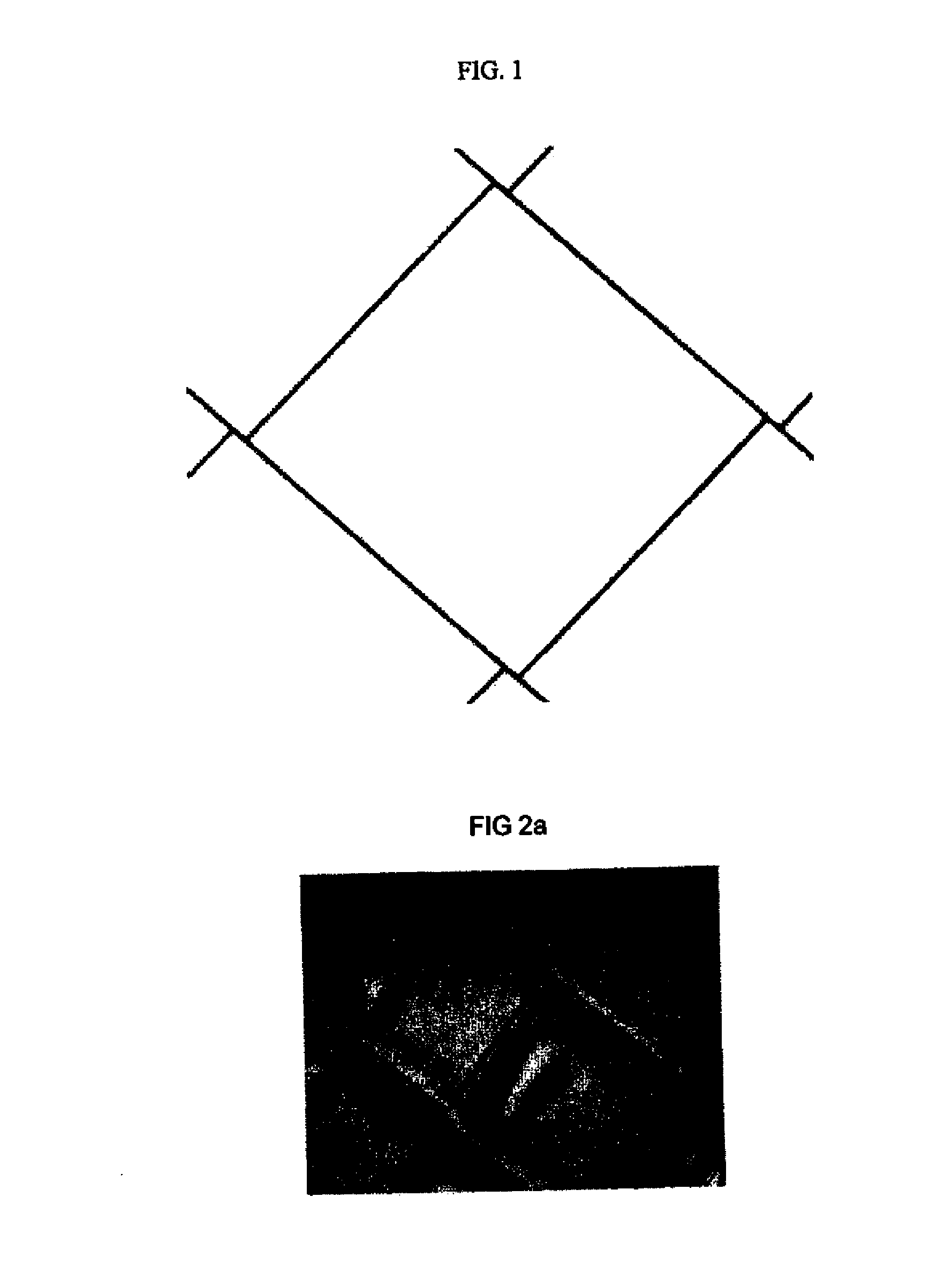
[0158]The dry film photoresist was then used make an imprint pattern in a similar manner to that described above in Invention Example 1. The transparent elastomeric mold used contained 16 measurement cells. Each measurement cell was about 102.3 mm long and 3.78 mm wide and was made with the connected diamond structure shown in FIG. 1. Therefore each measurement cell was about 170.5 diamond patterns long and...


PUM

PropertyMeasurementUnit
softening pointaaaaaaaaaa
widthaaaaaaaaaa
widthaaaaaaaaaa

Abstract

A photocurable composition includes an acid-generating compound, a multifunctional epoxy resin, and an epoxysilane oligomer represented by the following Structure (I):
wherein R1 is a substituted or unsubstituted alkyl group, R2 is a substituted or unsubstituted linear, branched, or cyclic alkyl group or an alkyl ether residue substituted with an epoxide, R3 is hydrogen or a substituted or unsubstituted alkyl, and x+y≧2. The photocurable composition can be provided as a photoresist layer on a substrate, and can then be imprinted to form a pattern of micro-channels. These micro-channels can be filled with a conductive composition (ink) and used to form an entrenched pattern of micro-wires to provide a transparent conductive electrode.

Description

CROSS REFERENCE TO RELATED APPLICATIONS[0001]Reference is made to commonly assigned, co-pending U.S. patent application Ser. No. ______ (Attorney Docket K001521) filed concurrently herewith by Wang, Lebens, and Wright and entitled “METHOD OF FORMING CONDUCTIVE FILMS WITH MICRO-WIRES,” the disclosure of which is incorporated herein by reference.[0002]Reference is also made to the following commonly assigned and copending patent applications:[0003]U.S. Ser. No. 13 / 746,346 filed Jan. 22, 2013 by Lebens et al.;[0004]U.S. Ser. No. 13 / 746,352 filed Jan. 22, 2013 by Lebens et al.;[0005]U.S. Ser. No. 13 / 757,891 filed Feb. 4, 2013 by Wang et al.;[0006]U.S. Ser. No. 13 / 757,896 filed Feb. 4, 2013 by Wang et al.;[0007]U.S. Ser. No. 13 / 757,899 filed Feb. 4, 2013 by Wang et al.;[0008]U.S. Ser. No. 13 / 757,901 filed Feb. 4, 2013 by Wang et al.;[0009]U.S. Ser. No. 13 / 757,905 filed Feb. 4, 2013 by Wang et al.; and[0010]U.S. Ser. No. 13,757,913 filed Feb. 4, 2013 by Wang et al.;[0011]the disclosures o...

Claims


Application Information

Patent Timeline
Patent Type & Authority Applications(United States)
IPC IPC(8): C08G59/02H05K1/09B29C59/00H05K1/02C08L63/00H01B1/20
CPCC08G59/02C08L63/00H01B1/20B29C59/00B29K2505/00H05K1/097C08L2203/20B29K2063/00H05K1/0296G03F7/0002G03F7/0755G03F7/0757Y10T428/249921Y10T428/31663Y10T428/24802
Inventor WANG, YONGCAILEBENS, JOHN ANDREWDICILLO, JOHN
Owner EASTMAN KODAK CO
Why Eureka
Try Eureka