
Organic electroluminescent element, organic electroluminescent lighting device and organic electroluminescent display device

a technology of organic electroluminescent elements and lighting devices, which is applied in the direction of energy-saving lighting, other domestic articles, sustainable buildings, etc., can solve the problems of low light emission efficiency of the resultant element, low light emission efficiency of the element, and inability to mix materials uniformly, etc., to achieve high power efficiency, low driving voltage, and the effect of high light emission efficiency

Active Publication Date: 2015-03-19
MITSUBISHI CHEM CORP
View PDF2 Cites 7 Cited by
  • Summary
  • Abstract
  • Description
  • Claims
  • Application Information

AI Technical Summary

Benefits of technology

The present invention provides an organic electroluminescent element that can be driven at a low voltage and has high power efficiency. It can be used in various lighting devices, such as copiers, liquid-crystal displays, and markers, among others. The technical value of this element is extremely high.

Problems solved by technology

For the purpose of white emission mainly in lighting applications, there has been developed an element that uses plural luminescent materials; however, in an organic electroluminescent element containing three or more different kinds of luminescent materials, electric charges could not be uniformly given to the luminescent materials and positive or negative charges could reach only a part of the luminescent materials, and as a result, there occur some problems that the light emission efficiency may lower and the element durability may lower.
In a case where a luminescent layer is formed according to a wet film formation method like in the present invention, there may occur other problems that the materials could not be mixed uniformly owing to the difference in solubility between the charge-transporting material and the luminescent material, or the materials could not be uniformly precipitated during film formation or drying but the individual materials may aggregate so that the light emission efficiency of the resultant element may lower.
Further, owing to the difference in solubility between other materials than charge-transporting materials, for example, luminescent materials and others, the materials could not be mixed uniformly or some concentration distribution may occur during film formation, thereby providing still other problems of light emission efficiency, etc.
In particular, in case of using a few different kinds of luminescent materials and producing a white luminescent element by the wet film formation method through combination of emission wavelengths, when the materials could not be mixed and precipitated uniformly, there is a probability that the problem would provide some negative influence on not only the light emission efficiency, but also the light emission spectrum, repetitive reproducibility, etc.

Method used


Image

  • Organic electroluminescent element, organic electroluminescent lighting device and organic electroluminescent display device
  • Organic electroluminescent element, organic electroluminescent lighting device and organic electroluminescent display device
  • Organic electroluminescent element, organic electroluminescent lighting device and organic electroluminescent display device

Examples


example 1

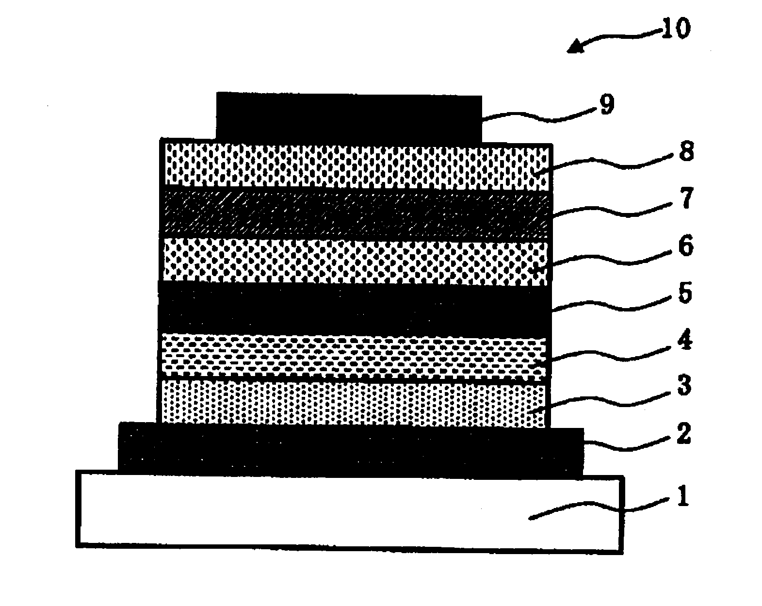
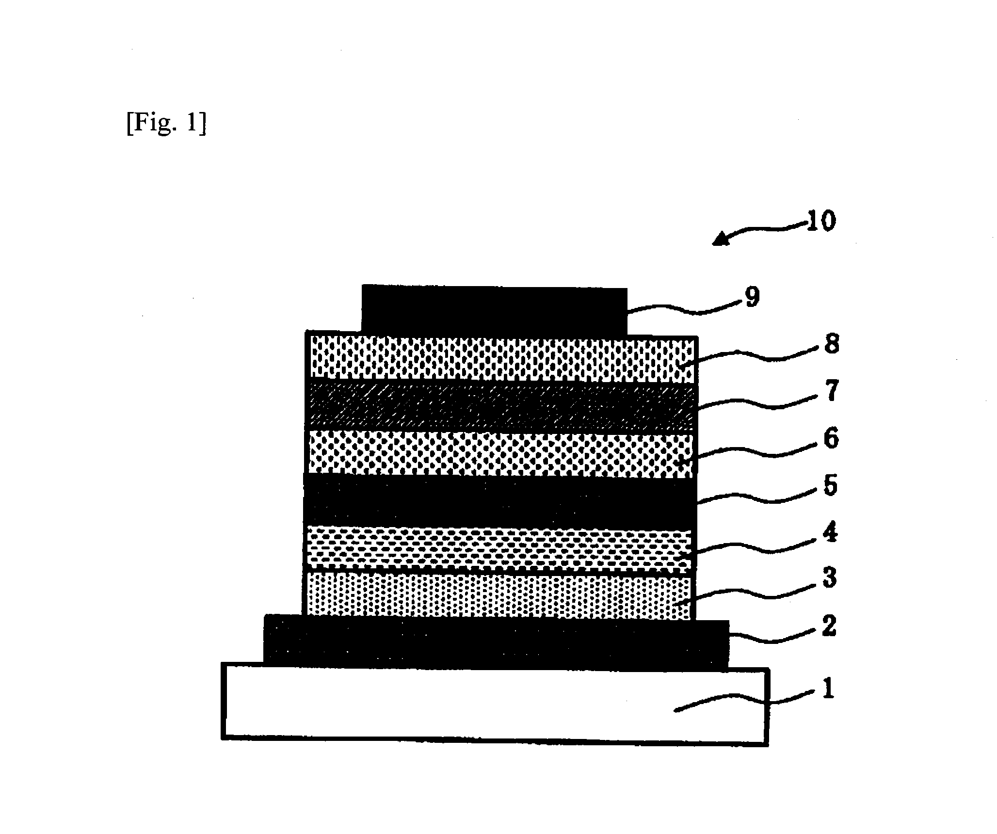
[0384]An organic electroluminescent element was produced according to the process mentioned below.

[0385]On a glass substrate 1 having, as deposited thereon by sputtering film formation, an indium tin oxide (ITO) transparent conductive film, an anode 2 was formed by patterning thereon in stripes each having a width of 2 mm, according to ordinary photolithography combined with hydrochloric acid etching. The thus-patterned ITO substrate was ultrasonically washed with an aqueous surfactant solution, washed with ultrapure water, ultrasonically washed with ultrapure water and then washed with ultrapure water in that order, then dried and further washed with UV ozone.

[0386]Next, a composition for forming hole injection layer was prepared, which has the following formulation and contains an arylamine polymer shown by the following structural formula (P-1), 4-isopropyl-4′-methyldiphenyliodonium tetrakis(pentafluorophenyl)borate shown by the structural formula (A-1) and ethyl acetate. The hol...

example 2

[0397]An organic electroluminescent element was produced in the same manner as in Example 1, except that a composition for forming luminescent layer containing the following compound (H-2) in addition to the compounds (H-1) and (E-1) as the charge-transporting materials therein and prepared to have the formulation mentioned below was used. The characteristics of the element are shown in Table 1.

SolventcyclohexylbenzeneComposition concentrationH-1: 1.313 wt %H-2: 1.313 wt %E-1: 0.875 wt %R1: 0.035 wt %G1: 0.0245 wt %B1: 0.35 wt %

example 3

[0398]An organic electroluminescent element was produced in the same manner as in Example 1, except that a composition for forming luminescent layer containing the following compound (H-3) in addition to the compounds (H-1) and (E-1) as the charge-transporting materials therein and prepared to have the formulation mentioned below using the following compound (B2) in place of the compound (B1) as the luminescent material was used. The characteristics of the element are shown in Table 1.

SolventcyclohexylbenzeneComposition concentration H-1: 1.313 wt %H-3: 1.313 wt %E-1: 0.875 wt %R1: 0.035 wt %G1: 0.0245 wt %B2: 0.35 wt %


PUM

PropertyMeasurementUnit
emission wavelengthsaaaaaaaaaa

Abstract

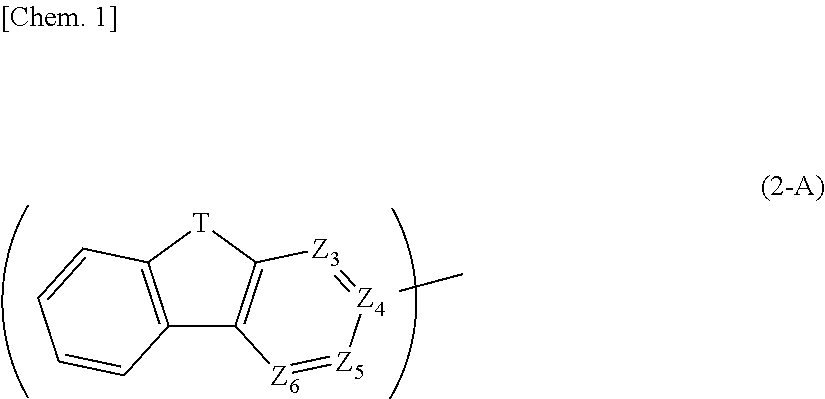
An organic electroluminescent element comprising: an anode; a cathode; a luminescent layer provided between the anode and the cathode; and a hole injecting and transporting layer provided between the anode and the cathode and adjacent to the luminescent layer, wherein at least the luminescent layer is formed by a wet film forming method, and contains a charge transporting material and a luminescent material, in which the charge transporting material contains a hole transporting material and an electron transporting material each having a specific partial structure, and the luminescent material contains at least three kinds of materials and has an emission spectrum having at least two kinds of emission maximums.

Description

TECHNICAL FIELD[0001]The present invention relates to an organic electroluminescent element, an organic electroluminescent lighting device and an organic electroluminescent display device.BACKGROUND ART[0002]Since the introduction of laminate-type organic electroluminescent (hereinafter this may be abbreviated as “EL”) elements into the market by Kodak using a vapor deposition method, organic EL displays have become actively developed and are now being put into practical use.[0003]The laminate-type organic electroluminescent element of the type comprises plural organic layers (luminescent layer, hole injection layer, hole transport layer, electron transport layer, etc.) as laminated between the anode and the cathode therein. The laminate-type organic electroluminescent element of the type is self-luminous and therefore has a broad viewing angle and high visibility, and in addition, it is thin and therefore attracts special attention from the viewpoint of space saving.[0004]Another c...

Claims


Application Information

Patent Timeline
Patent Type & Authority Applications(United States)
IPC IPC(8): H01L51/56H01L51/00H10K99/00
CPCH01L51/56H01L51/0073H01L51/0072H01L51/0067H01L51/0094H01L51/0074H01L51/0052H01L51/0035H01L51/0085H01L51/5056C07C211/54C07C211/61C07D401/14C07D403/10C07D403/14C07D405/10C07D405/14C07D409/14C09K11/06H05B33/14C09K2211/185C09K2211/1037C09K2211/1007C09K2211/1029C09K2211/1433C09K2211/1425C09K2211/1092C09K2211/1416H10K85/115H10K85/111H10K85/151H10K85/654H10K85/6574H10K85/342H10K85/6572H10K50/125H10K50/17H10K50/11H10K2101/10H10K2101/90Y02B20/00C07F15/00Y10S428/917H10K71/00H10K85/40H10K85/615H10K85/6576H10K50/15H10K50/16
Inventor TSURUTANI, YASUYUKIGOROHMARU, HIDEKIIMADA, ICHIRO
Owner MITSUBISHI CHEM CORP
Learn More