

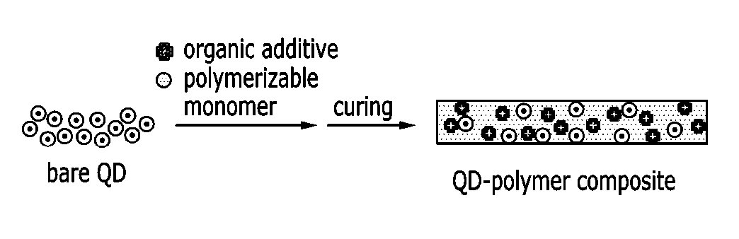
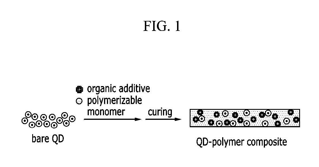
Nanocrystal polymer composites and production methods thereof
a technology of nanocrystals and composites, applied in the direction of instruments, non-metal conductors, conductors, etc., can solve the problems of insufficient uniform brightness, color purity may decrease, and the use of ccfl may not be guaranteed, so as to achieve enhanced brightness, high stability, and effective suppression of aggregation of nanocrystals
- Summary
- Abstract
- Description
- Claims
- Application Information
AI Technical Summary
Benefits of technology
Problems solved by technology
Method used
Image

Examples
reference example 1
Production of Bare Semiconductor Nanocrystals
[0262](1) 0.2 mmol of indium acetate, 0.6 mmol of palmitic acid, and 10 mL of 1-octadecene are placed in a flask, subjected to a vacuum state at 120° C. for one hour, and then heated to 280° C. after the atmosphere in the flask is exchanged with N2. Then, a mixed solution of 0.1 mmol of tris(trimethylsilyl)phosphine (TMS3P) and 0.5 mL of trioctylphosphine (TOP) is quickly injected and the reaction proceeds for 20 minutes. The reaction mixture then is rapidly cooled and acetone is added thereto to produce nanocrystals, which are then separated by centrifugation and dispersed in toluene. The first absorption maximum in UV-VIS spectrum of the InP core nanocrystals thus prepared is in the range of 420-600 nm.
[0263]0.3 mmol (0.056 g) of zinc acetate, 0.6 mmol (0.189 g) of oleic acid, and 10 mL of trioctylamine are placed in a flask, subjected to a vacuum state at 120° C. for 10 minutes, and then heated to 220° C. after the atmosphere in the fl...
preparation examples 3 to 6
Preparation of Semiconductor Nanocrystal Composition II
[0277]A semiconductor nanocrystal composition is prepared in the same manner set forth in Preparation Example 1, except using 0.37 wt % of oleyl amine (Preparation Example 3), 0.18 wt % of octyl amine (Preparation Example 4), 0.34 wt % of dioctyl amine (Preparation Example 5), and 2.5 wt % of trioctyl phosphine oxide (Preparation Example 6).
examples 3 to 6
[0278]A semiconductor nanocrystal—polymer composite is prepared in the same manner set forth in Example 1, except using the semiconductor nanocrystal compositions of Preparation Examples 3 to 6. The brightness of each film is measured and the results are shown in FIG. 5 and Table 3.
TABLE 3Organic additive (amount)haze (%)brightness (%)Example 3Oleyl amine (0.37 wt %)64.776Example 4Octyl amine (0.18 wt %)74.979Example 5Dioctyl amine (0.34 wt %)—84Example 6Trioctylphosphine oxide87.884(2.5 wt %)
[0279]The results of FIG. 5 and Table 3 confirm that the addition of the organic additive makes it possible to increase the brightness of the semiconductor nanocrystal—polymer composite film by about at least 2 times.
PUM
| Property | Measurement | Unit |
|---|---|---|
| haze | aaaaa | aaaaa |
| photoluminescence quantum yield | aaaaa | aaaaa |
| full width at half maximum | aaaaa | aaaaa |
Abstract
Description
Claims
Application Information