Conductive nanowire films

a technology of conductive nanowires and nanowires, which is applied in the field of conductive nanowire films, can solve the problems of increasing the price of indium, inability of the tcos family to meet the special requirements of the new generation device, and inability to fully integrate with the novel plastic based flexible opto-electronic device, etc., and achieves the effects of improving conductivity, flexibility, and improving features

Active Publication Date: 2015-04-16
P V NANO CELL +1
View PDF4 Cites 19 Cited by
  • Summary
  • Abstract
  • Description
  • Claims
  • Application Information

AI Technical Summary

Benefits of technology

[0020]Conductive films (in the nanometric or micrometric range), in particular transparent and conductive films are vastly used in the electronic, solar cells and opto-electronic industries and there is a continuous demand for films with improved features, i.e., conductivity, durability, flexibility as well as transparency and scaled down films. The present invention provides conductive films composed of stacked layers of nanowires, demonstrating improved properties, as further detailed hereinbelow.
[0054]The nanowire film additionally has high transparency to light due to the low volume filling of the metal in the film, namely the occupation of overall only a small surface area by the nanowires. The nanowire film is transparent between 400-800 nm. In some embodiment, the nanowires film is transparent homogenously, enabling production of reliable large scale films having about the same transparency value at each measurement point throughout the film. It should be understood that the term “homogeneously transparent film” or “uniform transparent film” refers to a film having about the same transparency at most regions in the film. The term “about the same transparency” as referred herein means transparency values which may fluctuate within the range of ±5% or ±10% or ±20% of the comparable value. The term “most of the areas” as referred herein means above 90% or above 80% or above 70% of the total film area (or total film area, which is covered with nanowires).
[0186]For some applications it may be necessary to embed the nanowire film in a solid matrix, with portions of the nanowires extending from the matrix to enable access to a conductive network. Such a matrix may provide protection to the nanowires from adverse factors such as corrosion and abrasion. The matrix may also offer mechanical properties to the conductive nanowire layer.
[0187]Additionally, performance-enhancing layers may be used to further enhance the characteristics of the nanowire film. This, for example, may be achieved by introducing additional layers in the transparent conductor structure of the invention. Thus, in other embodiments, the invention also provides a multi-layer transparent conductor which comprises the conductive nanowire film of the invention and at least one additional layer selected from an anti-reflective layer, an anti-glare layer, an adhesive layer, a barrier layer, and a protective coat.
[0190]For certain applications, the nanowire film may be treated, during manufacture or after it has been formed with a polymeric surfactant such as a cationic polymeric surfactant, so as to endow the nanowires or the film as a whole with increased physical stability. In some embodiments, the polymeric surfactant is poly-diallyldimethylammonium chloride. Alternatively, polymerizable monomers, such as styrene, that can be polymerized after film drying and nanowire formation using a polymerization initiator solution may be employed.

Problems solved by technology

First, the ever-increasing price of indium and the deposition process drove the continuous effort to find inexpensive substitutes with similar unique physical properties of high transparency along with low sheet resistivity, and second, the inability of the TCOs family in meeting the special requirements of the new generation devices.
For instance, TCOs are not fully compatible with novel plastic based flexible opto-electronic devices.
Moreover, their production does not include a high vacuum deposition step, as do traditional TCOs.
In addition, the traditional deposition methods are often incompatible with the emerging organic semiconductor based devices such as light emitting diodes or transistors due to sensitivity of the organic material to the sputter-coating process.

Method used


Image

  • Conductive nanowire films
  • Conductive nanowire films
  • Conductive nanowire films

Examples


Embodiment Construction

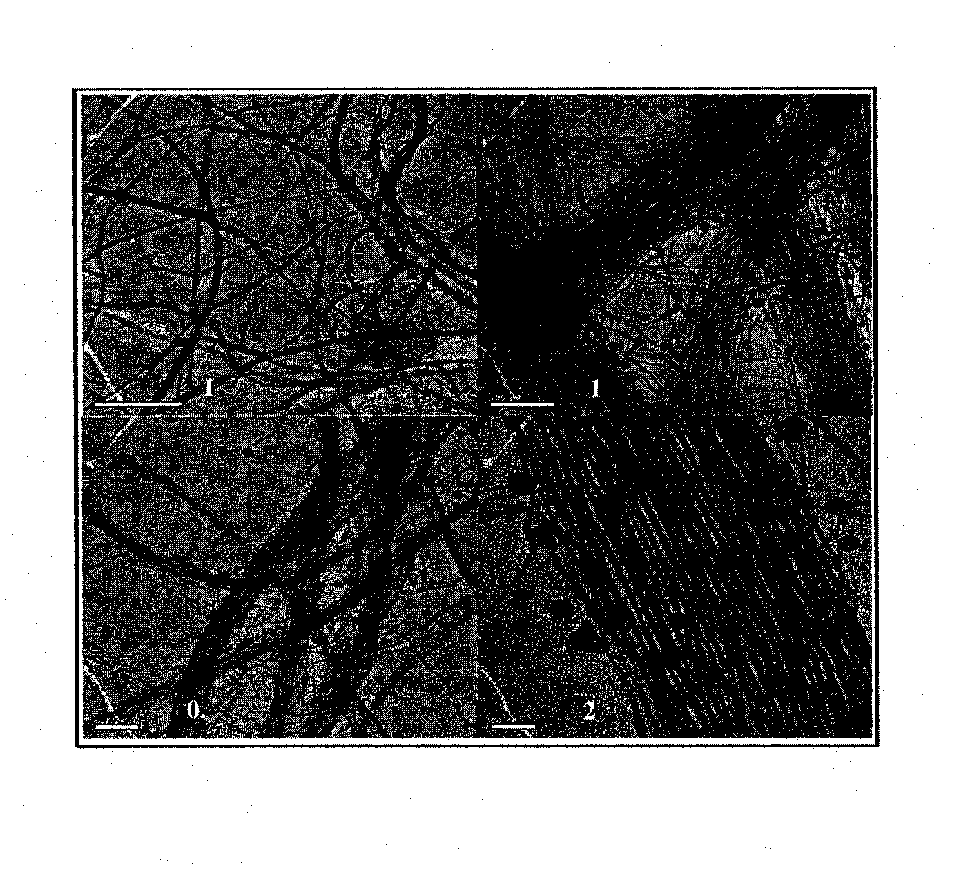
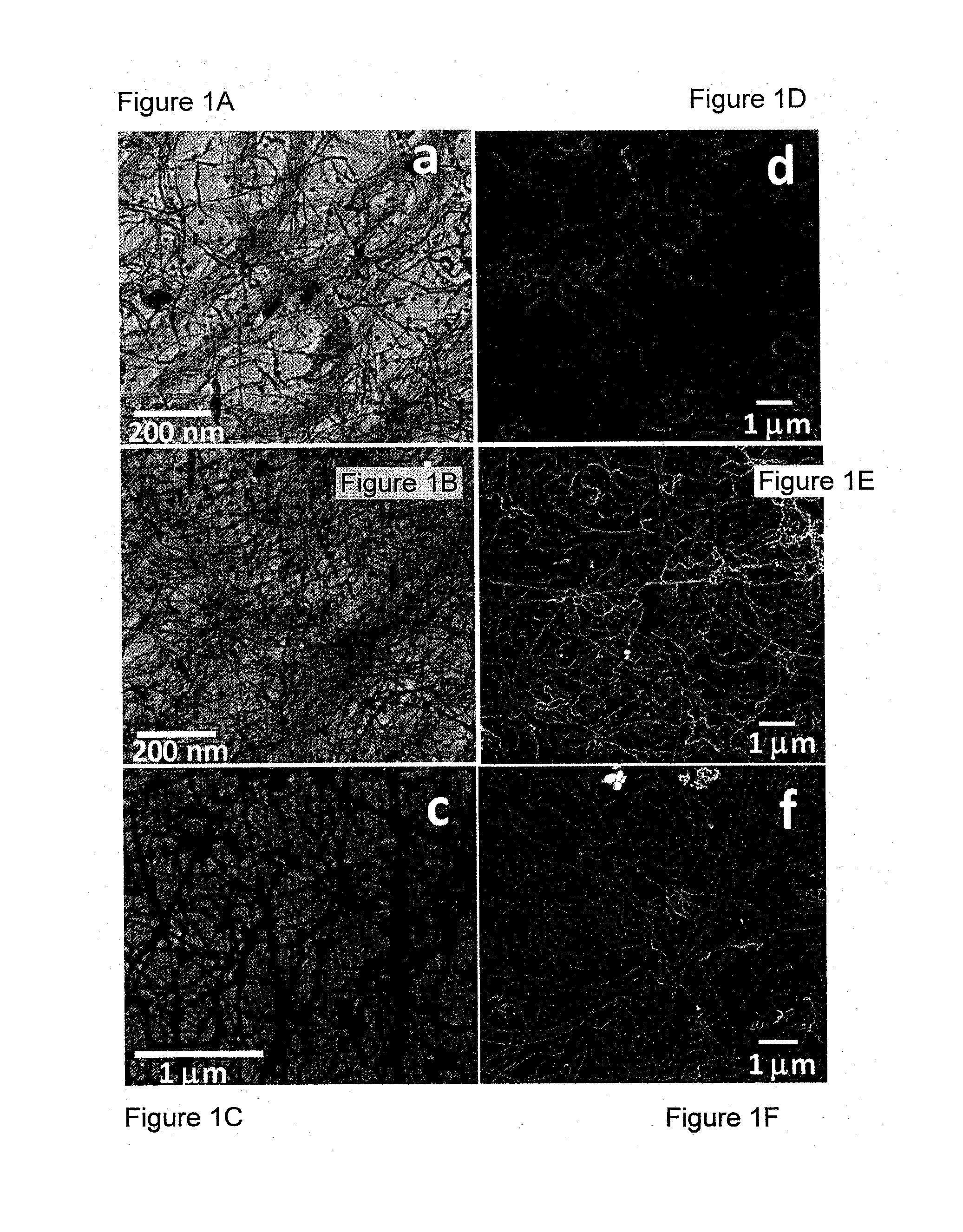
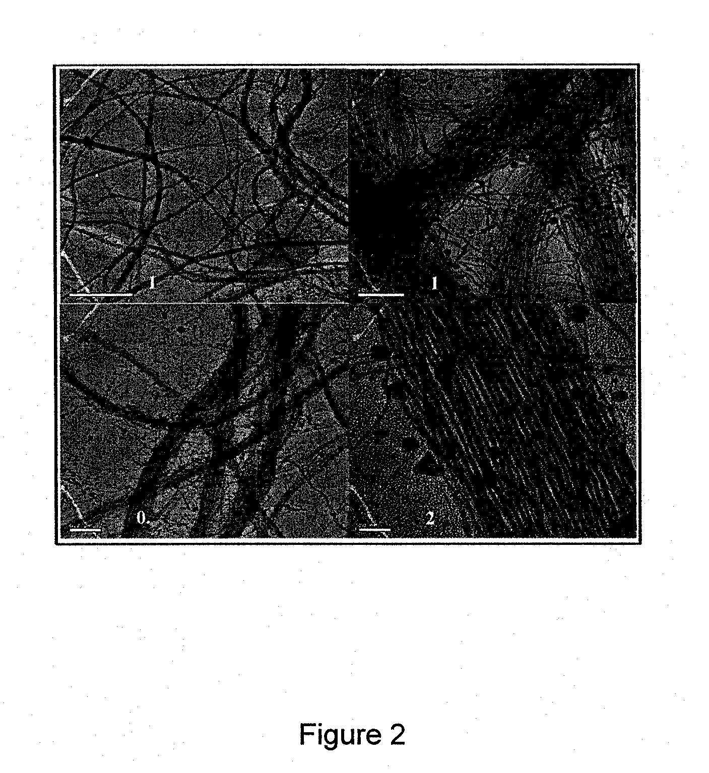
[0210]Conductive and transparent devices made of two or more layers of high aspect ratio nanowires clusters have been prepared in accordance with the processes of the invention. The transparent and conductive devices demonstrated the following properties: a sheet resistance of 100 Ω / square and light transmission in the visible range of about 85%.

PART A: Multilayer Film of Nanowires

Procedure 1: A Multilayer Film on a PET Substrate

[0211]An aqueous solution (10 ml) of cetyltrimethylammonium bromide (CTAB) (0.25M) at 35° C. was mixed with 500 μl of 25 mM tetrachloroauric acid (HAuCl4.3H2O) solution and 250 μl of 100 mM silver nitrate (AgNO3) solution. The 425 μl of 1.82M sodium ascorbate solution was added. As a result, the solution color changed from a yellow-brown to colorless. The final step involved the addition of 64 μl of sodium borohydride (NaBH4) solution (20 μM) Immediately after the addition of the NaBH4 the solution was deposited on a substrate and was left for about 30 min; ...


PUM

PropertyMeasurementUnit
distanceaaaaaaaaaa
distanceaaaaaaaaaa
distanceaaaaaaaaaa

Abstract

The invention provides a novel conductive film and a multilayered conductive structure, comprising a plurality of metal nanowires arranged in clusters and having an average aspect ratio of least 100,000, optionally decorated by metal nanoparticles. It is also disclosed a process for preparation of a conductive film comprising metal nanowires by surfactant / template assisted method which involves the use of a precursor solution based on surfactant (such as CTAB), metal precursor (such as HAuC14 and AgN03) and reducing agent (such as metal borohydride or sodium ascorbate).

Description

FIELD OF THE INVENTION[0001]This invention generally relates to conductive nanowire films and uses thereof.BACKGROUND OF THE INVENTION[0002]The search for new transparent electrode (TE) materials that would replace the transparent conducting oxides (TCOs), e.g., indium tin oxide (ITO), zinc oxide (ZnO) and fluorine-doped tin oxide (SnO2:F), commonly employed for various opto-electronic applications, has been the focus of a series of extensive studies [1].[0003]This quest has been motivated by two main objectives. First, the ever-increasing price of indium and the deposition process drove the continuous effort to find inexpensive substitutes with similar unique physical properties of high transparency along with low sheet resistivity, and second, the inability of the TCOs family in meeting the special requirements of the new generation devices. For instance, TCOs are not fully compatible with novel plastic based flexible opto-electronic devices. In addition to inexpensive production ...

Claims


Application Information

Patent Timeline
Patent Type & Authority Applications(United States)
IPC IPC(8): H01L21/288H01L29/45
CPCH01L21/288H01L29/45B82Y40/00C23C18/44H01L31/022466H01L31/1884C23C18/1651C23C18/1662G02F1/13439G02F2202/36B82Y30/00Y10T428/249921H01B1/02Y02E10/50H10K50/805H01L31/022491
Inventor MARKOVICH, GILAZULAI, DANIELLEVI-BELENKOVA, TATYANAGILON, HAGITDE LA VEGA, FERNANDOKABLA, AYALA
Owner P V NANO CELL
Why Eureka
Try Eureka