Radiation hardened mos devices and methods of fabrication
- Summary
- Abstract
- Description
- Claims
- Application Information
AI Technical Summary
Benefits of technology
Problems solved by technology
Method used
Image
Examples
Embodiment Construction
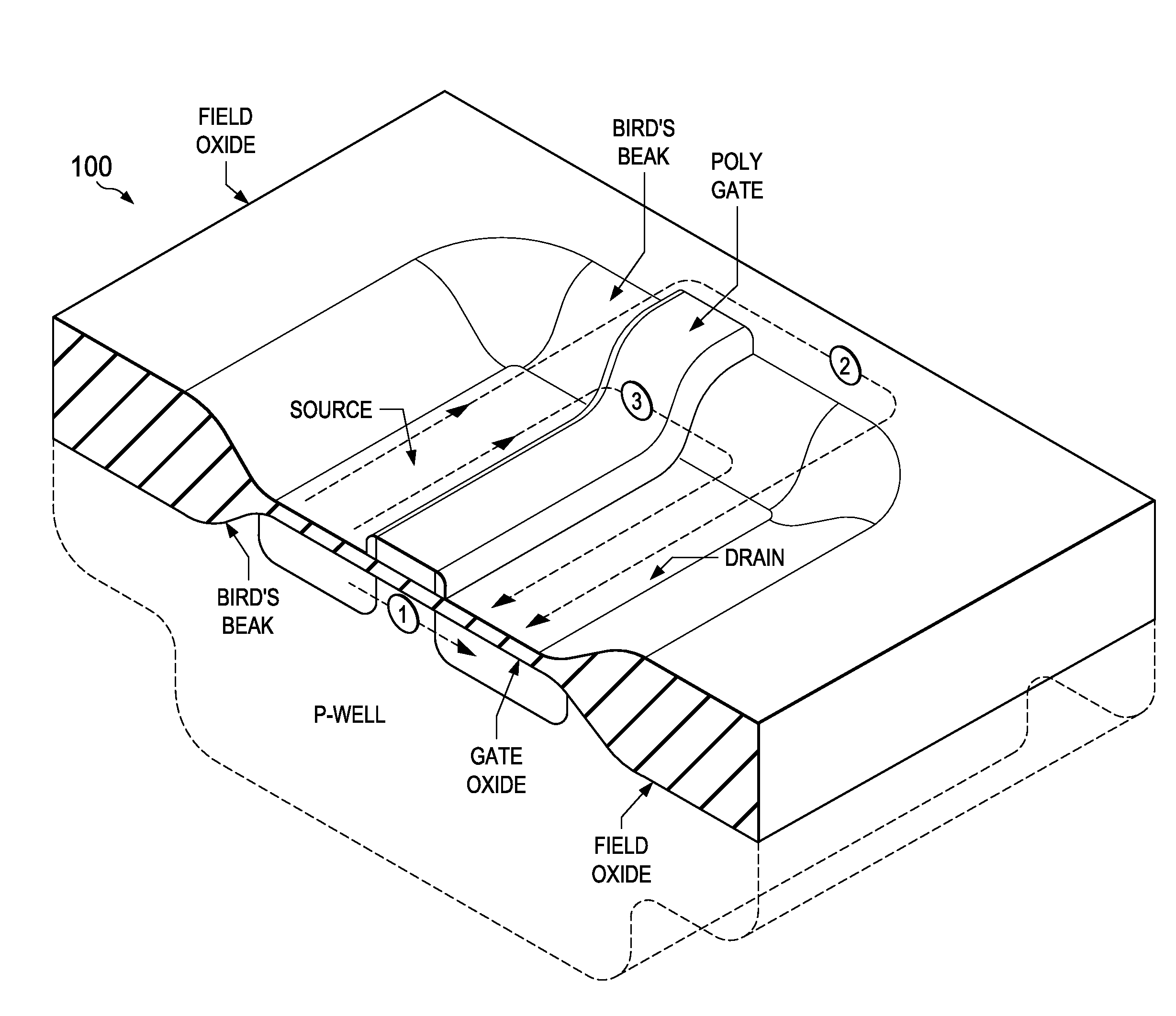
[0033]Referring to FIG. 1, there is shown a cross-sectioned isometric view of a typical NMOS transistor device 100 which can be part of an integrated circuit having multiple such transistors such as an NMOS device, a CMOS device (the PMOS transistor not being shown), or a BiCMOS device (which would additionally include bipolar junction transistors. In the illustrated device, the NMOS transistor is formed in a “p-well” which is a lightly doped p-type region formed within a silicon substrate. Alternatively, an entire top layer several micrometers thick or more of the silicon substrate can be lightly doped p-type material. The device 100 as illustrated in FIG. 1 is typical of one produced using a local oxidation of silicon (LOCOS) process used for isolating devices. It can be seen that a source and drain region are formed within a so-called “moat region” covered by a thin gate oxide, and surrounded by an isolating field oxide. Typical thicknesses for these oxides are in the range of 75...
PUM
 Abstract
Description
Claims
Application Information


