Method of manufacturing high resistivity soi wafers with charge trapping layers based on terminated si deposition

a technology of charge trapping layer and soi wafer, which is applied in the direction of semiconductor devices, semiconductor/solid-state device details, electrical apparatus, etc., can solve the problems of wasting one of the substrates, not having suitable thickness uniformity, and time-consuming and costly methods

Active Publication Date: 2015-04-30
GLOBALWAFERS CO LTD
View PDF3 Cites 158 Cited by
  • Summary
  • Abstract
  • Description
  • Claims
  • Application Information

AI Technical Summary

Benefits of technology

[0018]The present invention is still further directed to a method of preparing a silicon-on-insulator structure. The method comprises bonding an exposed front surface layer of a single crystal semiconductor handle structure and an exposed oxidized front surface of a single crystal silicon donor wafer. The single crystal semiconductor handle structure comprises (a) a single crystal semiconductor handle substrate comprising two major, generally parallel surfaces, one of which is a front surface of the single crystal silicon handle substrate and the other of which is a back surface of the single crystal silicon handle substrate, a circumferential edge joining the front and back surfaces of the single crystal silicon handle substrate, and a central plane of the single crystal silicon handle substrate between the front and back surfaces of the single crystal silicon handle substrate, wherein the single crystal silicon handle substrate has a minimum bulk resistivity of 100 Ohm-cm, (b) a multilayer in interfacial contact with the front surface dielectric layer, the multilayer comprising one or more passivated semiconductor layers, wherein the one or more passivated semiconductor layers comprise a polycrystalline or an amorphous structure and comprises a material selected from the group consisting of silicon, SiGe, SiC, and Ge, and (c) a semiconductor layer in interfacial contact with the multilayer, the semiconductor layer comprising a polycrystalline or an amorphous structure and comprises a material selected from the group consisting of silicon, SiGe, SiC, and Ge. The single crystal silicon donor wafer comprises two major, generally parallel surfaces, one of which is the exposed oxidized front surface of the single crystal silicon donor substrate and the other of which is a back surface of the single crystal silicon donor substrate, a circumferential edge joining the front and back surfaces of the single crystal silicon donor substrate, and a central plane of the single crystal silicon donor substrate between the front and back surfaces of the single crystal silicon donor substrate, wherein the single crystal silicon donor substrate comprises a cleave plane.
[0019]The present invention is still further directed to a single crystal semiconductor handle structure comprising a single crystal silicon handle substrate comprising two major, generally parallel surfaces, one of which is a front surface of the single crystal silicon handle substrate and the other of which is a back surface of the single crystal silicon handle substrate, a circumferential edge joining the front and back surfaces of the single crystal silicon handle substrate, and a central plane of the single crystal silicon handle substrate between the front and back surfaces of the single crystal silicon handle substrate, wherein the single crystal silicon handle substrate has a minimum bulk resistivity of 100 Ohm-cm; a multilayer in interfacial contact with the front surface layer, the multilayer comprising one or more passivated semiconductor layers, wherein the one or more passivated semiconductor layers comprise a polycrystalline or an amorphous structure and comprises a material selected from the group consisting of silicon, SiGe, SiC, and Ge; and a semiconductor layer in interfacial contact with the multilayer, the semiconductor layer comprising a polycrystalline or an amorphous structure and comprises a material selected from the group consisting of silicon, SiGe, SiC, and Ge.

Problems solved by technology

This method is time-consuming and costly, wastes one of the substrates and generally does not have suitable thickness uniformity for layers thinner than a few microns.
Concurrently with the heating or annealing of the bonded wafer, the particles earlier implanted in the donor wafer weaken the cleave plane.
Exposure to the elevated temperature causes initiation and propagation of a crack along the cleave plane, thus separating a portion of the donor wafer.
To reduce parasitic power loss and minimize harmonic distortion inherent when using conductive substrates for high frequency applications it is necessary, but not sufficient, to use substrate wafers with a high resistivity.
Such a substrate is prone to formation of high conductivity charge inversion or accumulation layers 12 at the BOX / handle interface causing generation of free carriers (electrons or holes), which reduce the effective resistivity of the substrate and give rise to parasitic power losses and device nonlinearity when the devices are operated at RF frequencies.
A problem that arises with these methods is that the defect density in the layer and interface tend to anneal out and become less effective at charge trapping as the wafers are subjected to the thermal processes required to make the wafers and build devices on them.
The charge trapping efficiency of these films becomes very poor.

Method used


Image

  • Method of manufacturing high resistivity soi wafers with charge trapping layers based on terminated si deposition
  • Method of manufacturing high resistivity soi wafers with charge trapping layers based on terminated si deposition
  • Method of manufacturing high resistivity soi wafers with charge trapping layers based on terminated si deposition

Examples


example 1

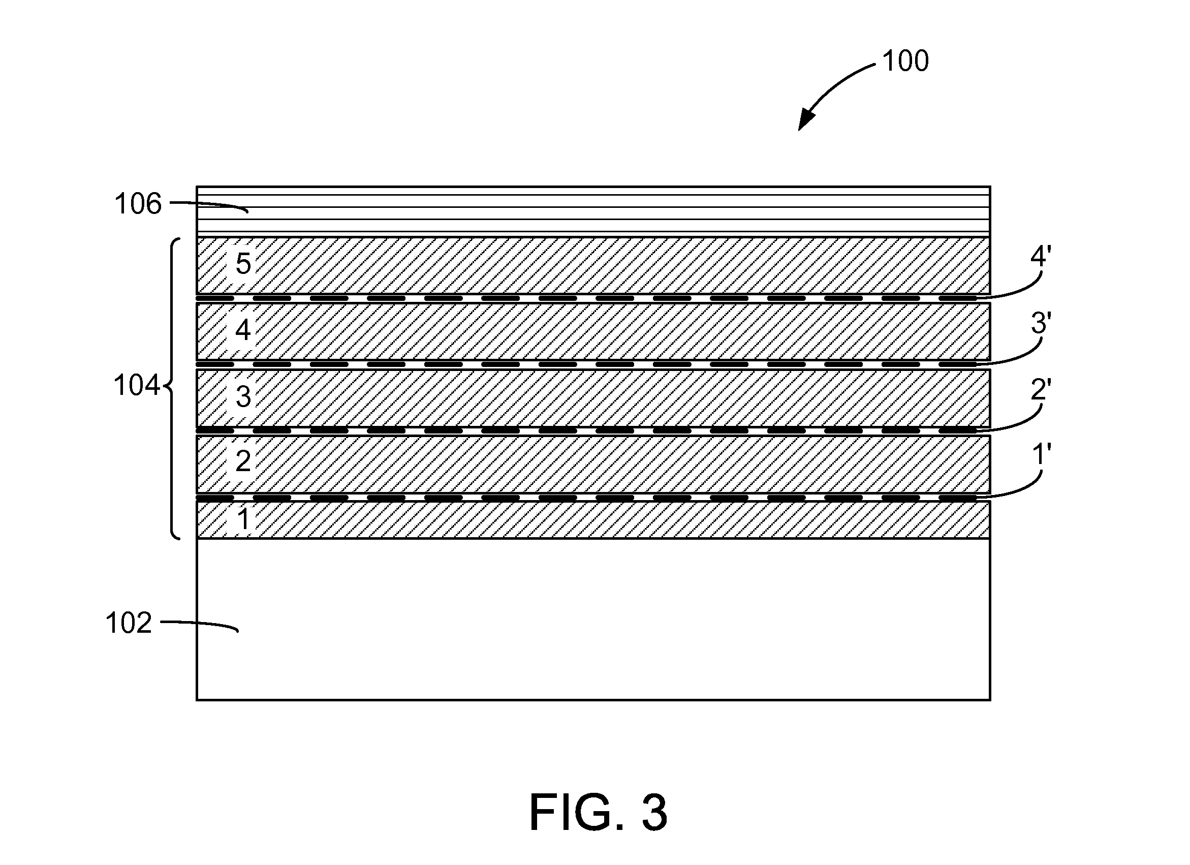
[0056]A multilayer structure 100 of the invention is illustrated in FIG. 3. The multilayer structure 100 comprises a high resistivity silicon substrate 102, a charge trapping layer 104, and a CVD oxide layer 106. The CVD oxide layer 106 deposited in a chemical vapor deposition (CVD) system. The charge trapping layer 104 comprises multiple passivated layers 1, 2, 3, 4, and 5 of amorphous silicon, each of the layers separated by an interim layers 1′, 2′, 3′, and 4′. Preparation of the multilayer structure 100 was according to the following protocol.

[0057]200 mm single side polished high resistivity single crystal silicon wafer substrate 102 with resistivity >750 Ohm-cm (SunEdison, Inc.; St. Peters, Mo.) was subjected to thermal oxidation to prepare a silicon oxide layer on the front surfaces of the wafer substrate 102. A charge trapping layer 104 comprising amorphous silicon was deposited on the oxidized surface with multiple termination and exposure to N2 atmosphere. The amorphous si...

example 2

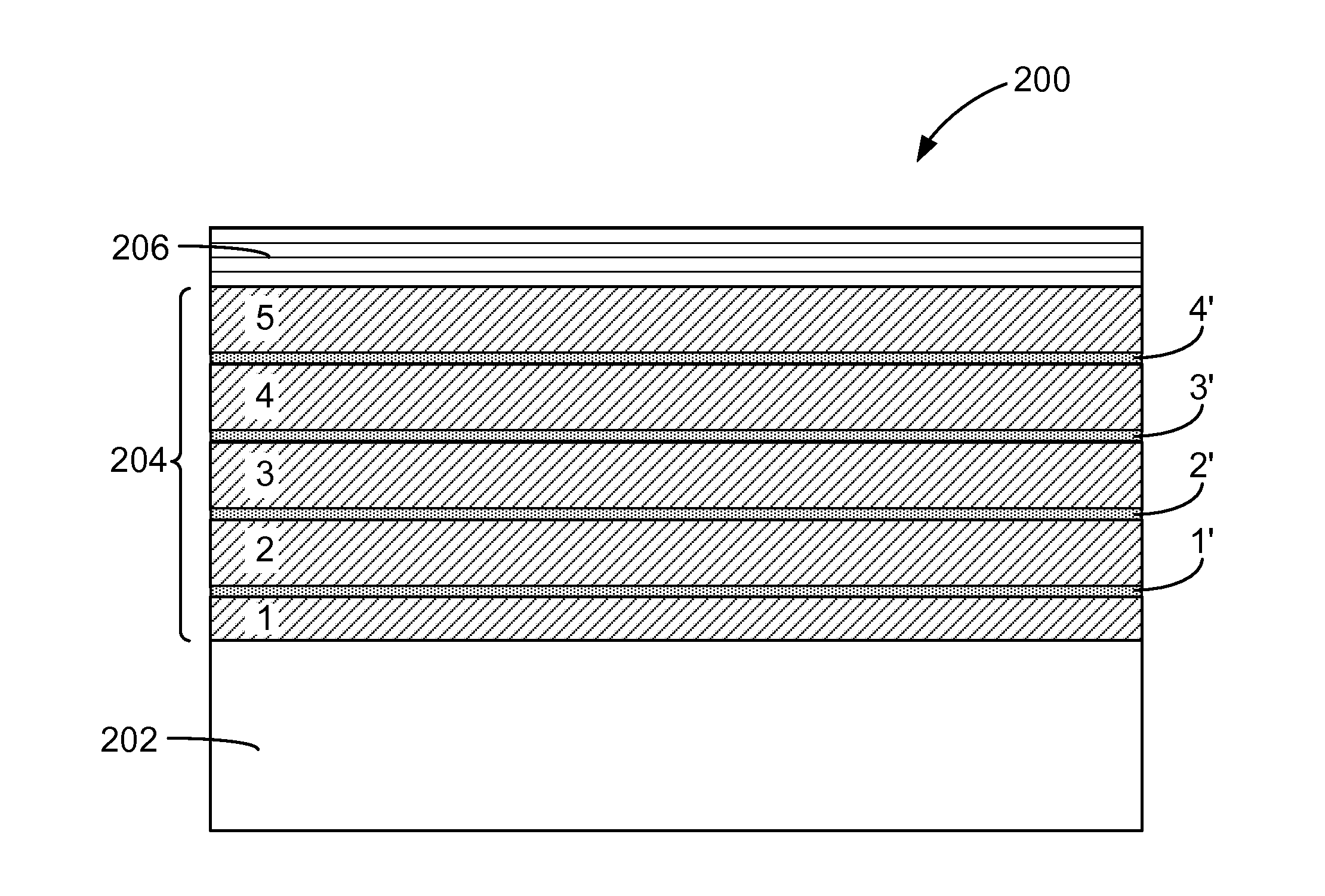
[0065]A multilayer structure 200 of the invention is illustrated in FIG. 4. The multilayer structure 200 comprises a high resistivity silicon substrate 202, a charge trapping layer 204, and a CVD oxide layer 206. The CVD oxide layer 206 deposited in a chemical vapor deposition (CVD) system. The charge trapping layer 204 comprises multiple passivated layers 1, 2, 3, 4, and 5 of amorphous silicon, each of the layers separated by an oxide layer 1′, 2′, 3′, and 4′. Preparation of the multilayer structure 200 was according to the following protocol.

[0066]200 mm single side polished single crystal silicon wafer substrate 202 with resistivity >750 Ohm-cm (SunEdison, Inc.; St. Peters, Mo.) were subjected to thermal oxidation to prepare a silicon oxide layer on the front surfaces of the wafers. A charge trapping layer 204 comprising amorphous silicon was deposited on the oxidized surfaces with multiple termination and exposure to O2 atmosphere. The amorphous silicon was deposited in LPCVD re...


PUM

PropertyMeasurementUnit
resistivityaaaaaaaaaa

Abstract

A method of preparing a single crystal semiconductor handle wafer in the manufacture of a silicon-on-insulator device is provided. The method comprises forming a multilayer of passivated semiconductors layers on a dielectric layer of a high resistivity single crystal semiconductor handle wafer. The method additionally comprises forming a semiconductor oxide layer on the multilayer of passivated semiconductor layers. The multilayer of passivated semiconductor layers comprise materials suitable for use as charge trapping layers between a high resistivity substrate and a buried oxide layer in a semiconductor on insulator structure.

Description

CROSS REFERENCE TO RELATED APPLICATION[0001]This application claims priority of U.S. Provisional Application No. 61 / 898,983 filed on Nov. 1, 2013 which is hereby incorporated by reference in its entirety.THE FIELD OF THE INVENTION[0002]The present invention generally relates to the field of semiconductor wafer manufacture. More specifically, the present invention relates to a method of preparing a handle substrate for use in the manufacture of a semiconductor-on-insulator (e.g., silicon-on-insulator) structure, and more particularly to a method for producing a charge trapping layer in the handle wafer of the semiconductor-on-insulator structure.BACKGROUND OF THE INVENTION[0003]Semiconductor wafers are generally prepared from a single crystal ingot (e.g., a silicon ingot) which is trimmed and ground to have one or more flats or notches for proper orientation of the wafer in subsequent procedures. The ingot is then sliced into individual wafers. While reference will be made herein to ...

Claims


Application Information

Patent Timeline
Patent Type & Authority Applications(United States)
IPC IPC(8): H01L21/762H01L29/16H01L21/02
CPCH01L21/76251H01L21/02592H01L21/02595H01L21/02532H01L29/16H01L21/02164H01L21/02238H01L21/02255H01L21/02529H01L21/0262
Inventor PEIDOUS, IGORPELLICANO, ILLARIA KATIA MARIANNA
Owner GLOBALWAFERS CO LTD
Why Eureka
Try Eureka