
Method for producing conductive substrate, conductive substrate, and organic electronic element

a technology of conductive substrates and organic electronic elements, applied in the direction of dielectric characteristics, sustainable manufacturing/processing, final product manufacturing, etc., can solve the problems of low heat resistance, many steps in the photoresist process, and the conductive substrates are discarded most of the time, and achieve less or no damage, high conductive

Inactive Publication Date: 2015-05-14
KONICA MINOLTA INC
View PDF2 Cites 4 Cited by
  • Summary
  • Abstract
  • Description
  • Claims
  • Application Information

AI Technical Summary

Benefits of technology

The patent describes a water-soluble binder resin that is compatible with a conductive polymer and can increase the thickness of the layer without reducing its conductivity and transparency. The resin can be dissolved in water and has a specific structure. The resin is preferably a copolymer with another monomer component. The resin is present in the conductive polymer layer in a certain content. The resin has a certain molecular weight and can be determined by GPC using a solvent like THF or DMF. The technical effect of the patent is to provide a way to increase the thickness of a conductive polymer layer without affecting its conductivity and transparency.

Problems solved by technology

However, such steps of patterning thin metal lines in the conventional photolithographic process waste most of a metal film for patterning and a resist material.
Furthermore, the photoresist process, which has many steps, has low throughput.
However, this method needs a heat treatment at 200° C. or more to anneal the metal nanoparticles to establish an electrically conducted pattern of metal nanoparticles, and thus cannot be readily applied to inexpensive resin bare substrates having low heat resistance.
A lower heat treating temperature to avoid thermal damage to the bare substrate requires a longer time for annealing of metal nanoparticles, resulting in low throughput.
The organic EL element cannot have high light extraction efficiency because the light partially reflects at interfaces between layers laminated to form the organic EL element, such as a bare substrate, electrodes, and a luminous layer, to be confined inside the element.

Method used


Image

  • Method for producing conductive substrate, conductive substrate, and organic electronic element
  • Method for producing conductive substrate, conductive substrate, and organic electronic element
  • Method for producing conductive substrate, conductive substrate, and organic electronic element

Examples


example 1

Preparation of Transparent Conductive Substrate ACF-1

(Formation of Patterned Thin Metal Lines)

[0203]A polyethylene terephthalate (PET) film (thickness: 110 μm, dimensions: 180 by 180 mm) provided with hard coat layers on both surfaces thereof was prepared. A pattern of thin metal lines was printed on one surface of the film by gravure printing with a silver nanoparticle ink (TEC-PR-030; available from InkTec Co., Ltd.). The printing was conducted through a gravure printing pattern of a square lattice having a width of 30 μm and a pitch of 0.75 mm such that the average height of the thin lines became 0.8 μm after annealing. A compact thick-film semi-automatic printing machine STF-1501P (available from Tokai Shoji Co., Ltd.) was used. The pattern was printed in an area of 150 square millimeters.

(Annealing of Patterned Thin Metal Lines)

[0204]After printing of the pattern of thin metal lines, the patterned thin metal lines were annealed on a hot plate at 120° C. for 30 minutes to prepar...

example 2

[0244]A sample was prepared as in Example 1 except that that the pattern of thin metal lines was formed with a silver complex ink (TEC-IJ-010; available from InkTec Co., Ltd.), and was printed by an inkjet process.

[0245]The sample was evaluated as in Example 1. The results are similar to those of Example 1.

example 3

Preparation of Organic EL Element AOL-30

(Preparation of Transparent Conductive Substrate ACF-30)

[0246]An ITO transparent conductive layer (average thickness: 150 nm, dimensions: 50 by 50 mm) was formed on one surface of a clean alkali-free glass bare substrate (thickness: 0.7 mm, dimensions: 80 by 80 mm) by sputtering in accordance with a standard method to prepare Transparent conductive substrate ACF-30.

[0247]Transparent conductive substrate ACF-30 had a transmittance of 84% and a sheet resistance of 12 Ω / sq.

(Preparation of Organic EL Element)

[0248]Transparent conductive substrate ACF-30 was used as a first electrode (anode), and Organic EL element AOL-30 was prepared by the following procedure.

[0249]PEDOT-PSS CLEVIOS P AI 4083 (solid content: 15%) (available from Heraeus Holding GmbH) was applied onto the conductive surface of Transparent conductive substrate ACF-30 as the first electrode with an applicator (coating width: 50 mm) such that the dry thickness of the coating was 30 n...


PUM

PropertyMeasurementUnit
light transmittanceaaaaaaaaaa
transmittanceaaaaaaaaaa

Abstract

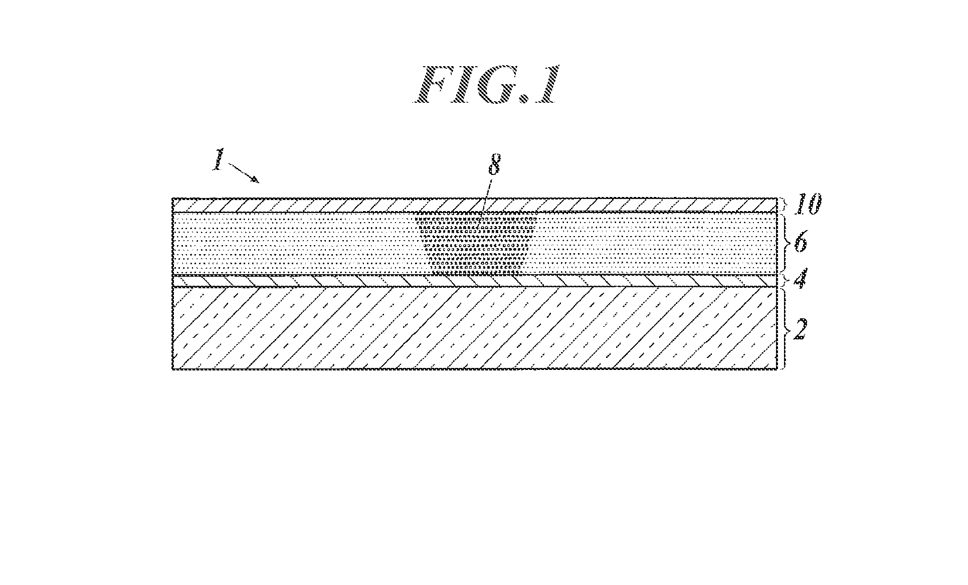
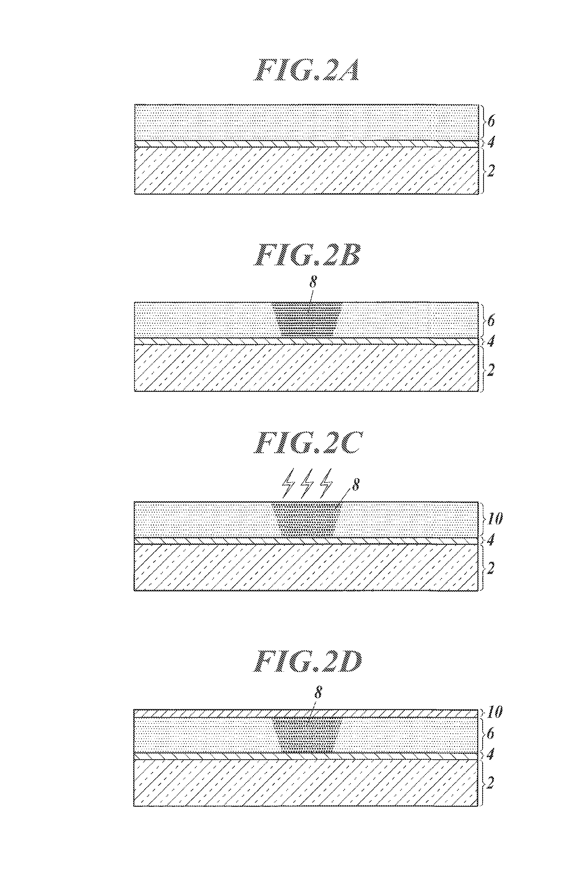
A method for producing a conductive substrate including at least an anchor layer and a pattern of conductive thin metal lines on a bare substrate is provided. The method includes the steps of: forming a porous anchor layer mainly composed of an inorganic compound on the bare substrate; forming the pattern of thin metal lines containing metal nanoparticles and a metal complex on the anchor layer; and performing thermal annealing of the pattern of thin metal lines by irradiation of flash light.

Description

TECHNICAL FIELD[0001]The present invention relates to a method for producing a conductive substrate, a conductive substrate, and an organic electronic element for an organic electronic device such as an organic electroluminescent (EL) device using the conductive substrate, and a solar cell.BACKGROUND ART[0002]There have been invented, as methods for producing conductive substrates having patterned thin metal lines, a subtractive method and an additive method, and they have been extensively used because of their high reliability. Conductive substrates have been recently used in a variety of electronic apparatuses / devices, and have required higher density of patterned thin metal lines to meet higher-performance apparatus / devices. These methods usually employ photolithographic processes suitable for microfabrication to form desired patterns of thin metal lines.[0003]In a photolithographic process, a resist is applied over an entire substrate, and the substrate is prebaked. The substrat...

Claims


Application Information

Patent Timeline
Patent Type & Authority Applications(United States)
IPC IPC(8): H01L51/00H05K1/03H05K1/02H05K3/10
CPCH01L51/0096H01L51/0022H05K3/10H05K2203/11H05K1/0271H01L51/44H01L51/52H05K1/0306H05B33/02H05B33/10H05K3/1283H05K2201/0108H05K3/1208H05K2201/0116Y02E10/549Y02P70/50H10K71/60H10K85/1135H10K77/111H10K50/814H10K2102/331H10K30/50H10K77/10H10K50/81H10K71/611H10K30/80H10K50/80
Inventor TAKADA, HIROSHIMATSUMURA, TOSHIYUKIGOTO, MASAKI
Owner KONICA MINOLTA INC
Learn More