Semiconductor device including gate structure for threshold voltage modulation in transistors and method for fabricating the same

a technology of threshold voltage modulation and semiconductor devices, which is applied in the direction of semiconductor devices, electrical equipment, transistors, etc., can solve the problems of difficult to form metal gate electrodes with n type work functions and p type work functions, increase gate leakage, and reduce so as to prevent the effective work function of the gate stack from being decreased, the threshold voltage of p channel transistors is reduced, and the effective work function of the gate stack is decreased

Active Publication Date: 2015-05-14
SK HYNIX INC
View PDF3 Cites 35 Cited by
  • Summary
  • Abstract
  • Description
  • Claims
  • Application Information

AI Technical Summary

Benefits of technology

[0011]According to the embodiments, since a dipole-interface and a P type work function gate electrode are included, it may be possible to decrease the threshold voltage of a P channel transistor.
[0012]Also according to the embodiments since a dipole interface and a thin N type work function gate electrode are included, it may be possible to decrease the threshold voltage of an N channel transistor.
[0013]Moreover, according to the embodiments, since a reaction preventing layer is formed on a P type work function gate electrode, it may be possible to substantially prevent the effective work function of a gate stack from being decreased from a subsequent process. In addition, because the reaction preventing layer is formed, and it is not necessary to remove a non-threshold voltage modulation layer and a non-work function layer, which are formed on the reaction preventing layer, a process may be simplified.

Problems solved by technology

If a transistor is scaled down to improve the performance thereof, gate leakage increases as the thickness of a gate dielectric layer becomes thin.
However, the introduction of the high-k material may have resulted in a Fermi level pinning effect.
However, it may be difficult to form metal gate electrodes with an N type work function and a P type work function, which require threshold voltages (Vt) appropriate for respective transistors, in a fabrication process of a CMOS device.

Method used


Image

  • Semiconductor device including gate structure for threshold voltage modulation in transistors and method for fabricating the same
  • Semiconductor device including gate structure for threshold voltage modulation in transistors and method for fabricating the same
  • Semiconductor device including gate structure for threshold voltage modulation in transistors and method for fabricating the same

Examples


first embodiment

[0035]FIGS. 1A and 1B are views explaining a method for threshold voltage modulation of a transistor in accordance with a

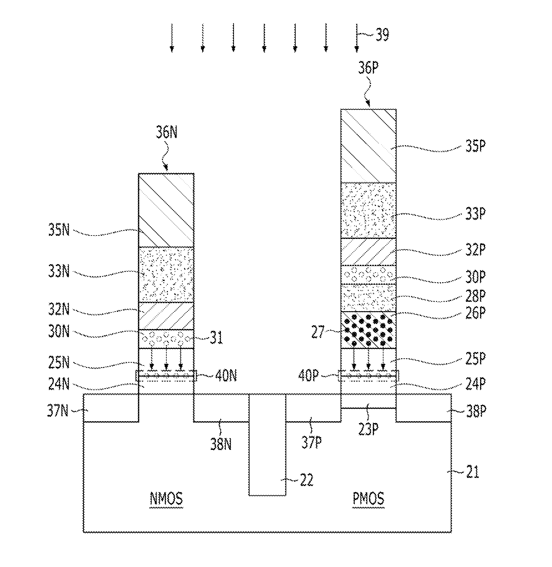
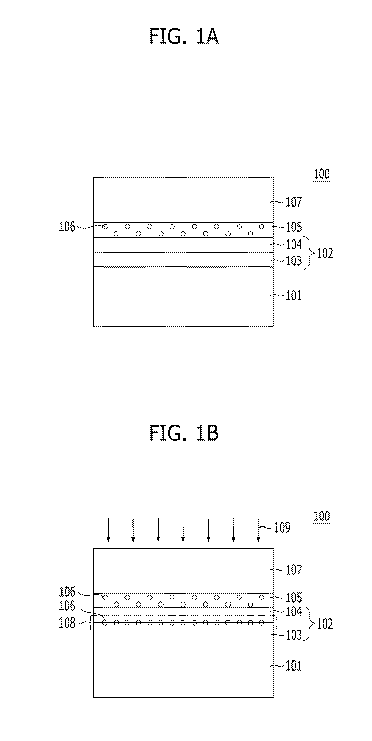
[0036]As shown in FIG. 1A, in order to form a transistor 100, a substrate 101 is prepared. The substrate 101 may include a silicon substrate.

[0037]A gate dielectric layer 102 is formed on the substrate 101. The gate dielectric layer 102 includes an interface layer 103 and a high-k dielectric layer 104.

[0038]A threshold voltage (Vt) modulation layer 105 is formed. The threshold voltage modulation layer 105 is a layer that contains a species 106 for modulating the threshold voltage of the transistor 100. The species 106 may include a lanthanum series element. The threshold voltage modulation layer 105 may include lanthanum oxide.

[0039]A gate electrode 107 is formed. The gate electrode 107 has an effective work function appropriate for the transistor 100. The gate electrode 107 includes a metal nitride. The gate electrode 107 includes titanium nitride.

[0040]As shown ...

second embodiment

[0042]FIGS. 2A and 2B are views explaining a method for threshold voltage modulation of a transistor in accordance with a

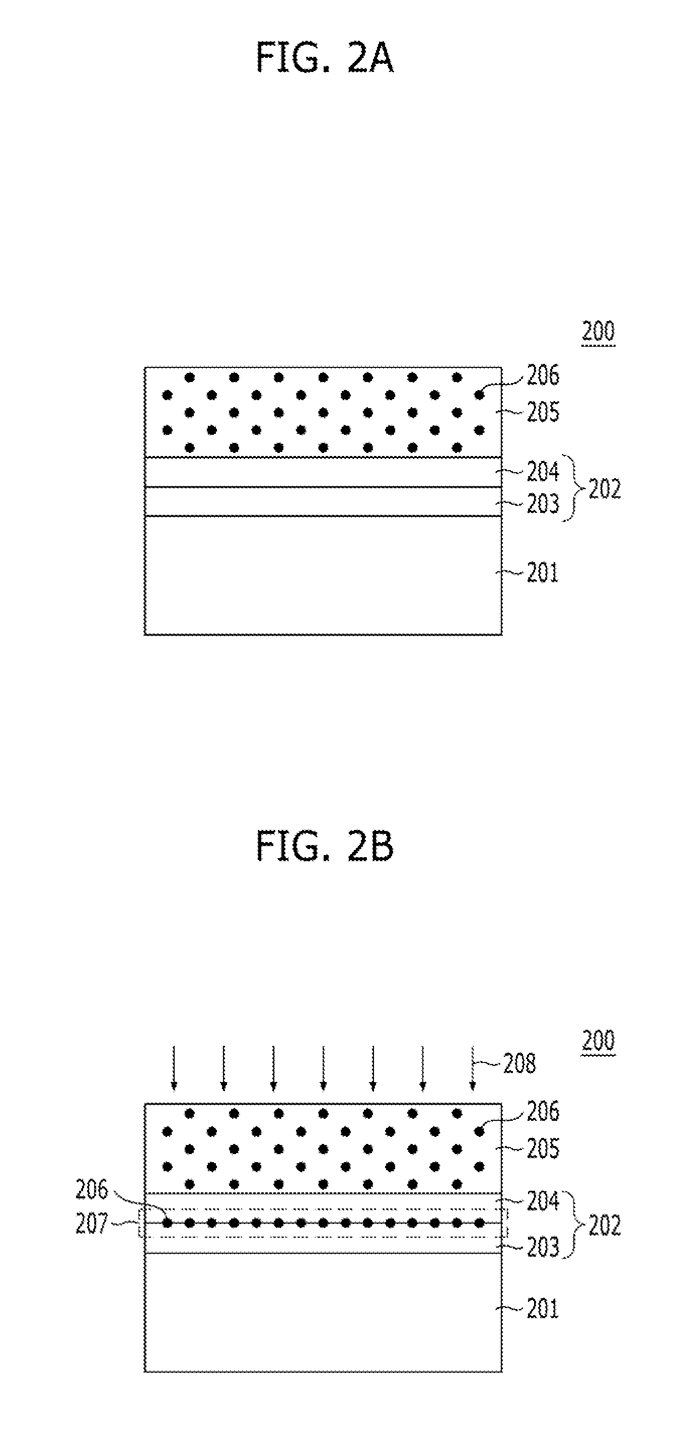
[0043]Referring to FIG. 2A, in order to form a transistor 200, a substrate 201 is prepared. The substrate 201 may include a silicon substrate.

[0044]A gate dielectric layer 202 is formed on the substrate 201. The gate dielectric layer 202 includes an interface layer 203 and a high-k dielectric layer 204.

[0045]A gate electrode 205 is formed on the gate dielectric layer 202. The gate electrode 205 has an effective work function appropriate for the transistor 200. The gate electrode 205 includes a species 206 for modulating the threshold voltage of the transistor 200. The species 206 may be doped into the gate electrode 205. The species 206 includes aluminum. The gate electrode 205 may include a titanium nitride layer that contains aluminum.

[0046]As shown in FIG. 2B, a dipole-interface 207 is formed in the gate dielectric layer 202. The dipole-interface 207 is formed ...


PUM


Abstract

A method for fabricating a semiconductor device includes forming an NMOS region and a PMOS region in a substrate, forming a first stack layer including a first gate dielectric layer and a first work function layer that is disposed over the first gate dielectric layer and contains aluminum, over the PMOS region of the substrate, forming a second stack layer including a second gate dielectric layer, a threshold voltage modulation layer that is disposed over the second gate dielectric layer and contains lanthanum, and a second work function layer that is disposed over the threshold voltage modulation layer, over the NMOS region of the substrate, and annealing the first stack layer and the second stack layer, thereby forming a first dipole-interface by diffusion of the aluminum in the first gate dielectric layer and a second dipole-interface by diffusion of the lanthanum in the second gate dielectric layer, respectively.

Description

CROSS-REFERENCE TO RELATED APPLICATIONS[0001]The present application claims priority of Korean Patent Application No. 10-2013-0136842, filed on Nov. 12, 2013, which is incorporated herein by reference in its entirety.BACKGROUND[0002]1. Field[0003]Exemplary embodiments of the present invention relate to a semiconductor device, more particularly, to a semiconductor device including a gate structure for threshold voltage modulation in transistors, and a method for fabricating the same.[0004]2. Description of the Related Art[0005]If a transistor is scaled down to improve the performance thereof, gate leakage increases as the thickness of a gate dielectric layer becomes thin. In order to cope with this concern, the material of a gate dielectric layer is replaced with a high-k material that has a dielectric constant larger than the dielectric constant of SiO2. The high-k material may include a metal oxide containing hafnium, a metal oxide containing zirconium or the like. However, the int...

Claims


Application Information

Patent Timeline
Patent Type & Authority Applications(United States)
IPC IPC(8): H01L27/092H01L29/51H01L21/8238
CPCH01L27/0922H01L29/512H01L21/823857H01L21/823842H01L21/28202H01L29/4966H01L29/513H01L29/518H01L29/1054H01L27/092H01L21/18H01L29/517
Inventor JI, YUN-HYUCKJANG, SE-AUGLEE, SEUNG-MIKIM, HYUNG-CHUL
Owner SK HYNIX INC
Why Eureka
Try Eureka