
Method and apparatus for laser processing of silicon by filamentation of burst ultrafast laser pulses

Active Publication Date: 2015-06-04
ROFIN SINAR TECH
View PDF4 Cites 76 Cited by
  • Summary
  • Abstract
  • Description
  • Claims
  • Application Information

AI Technical Summary

Benefits of technology

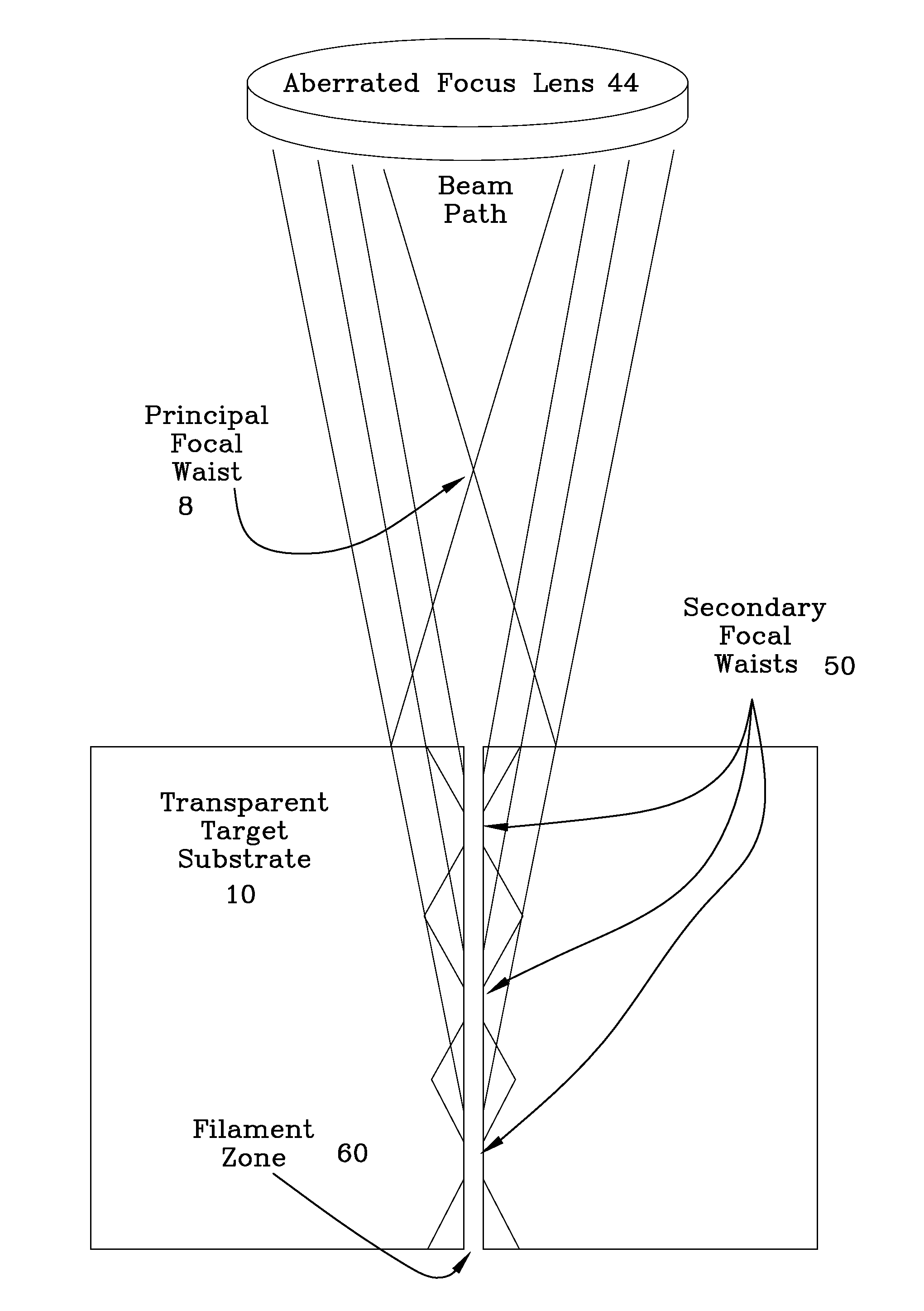
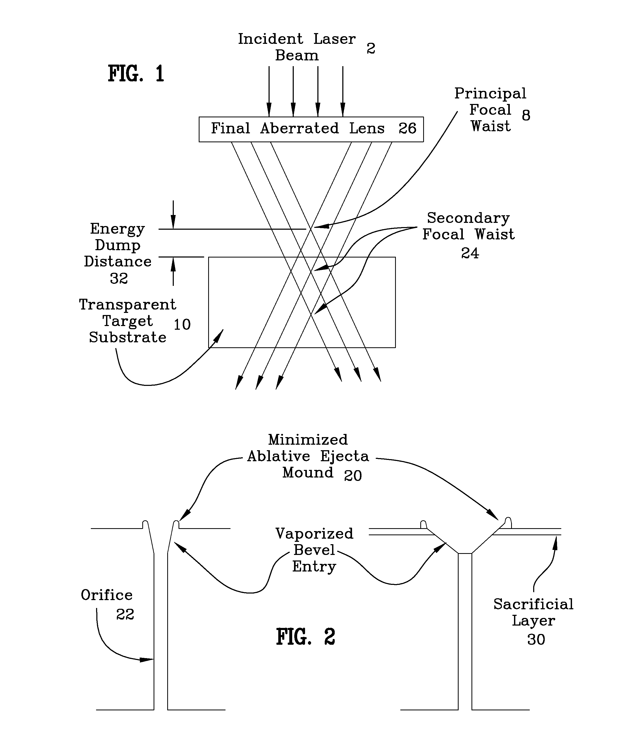
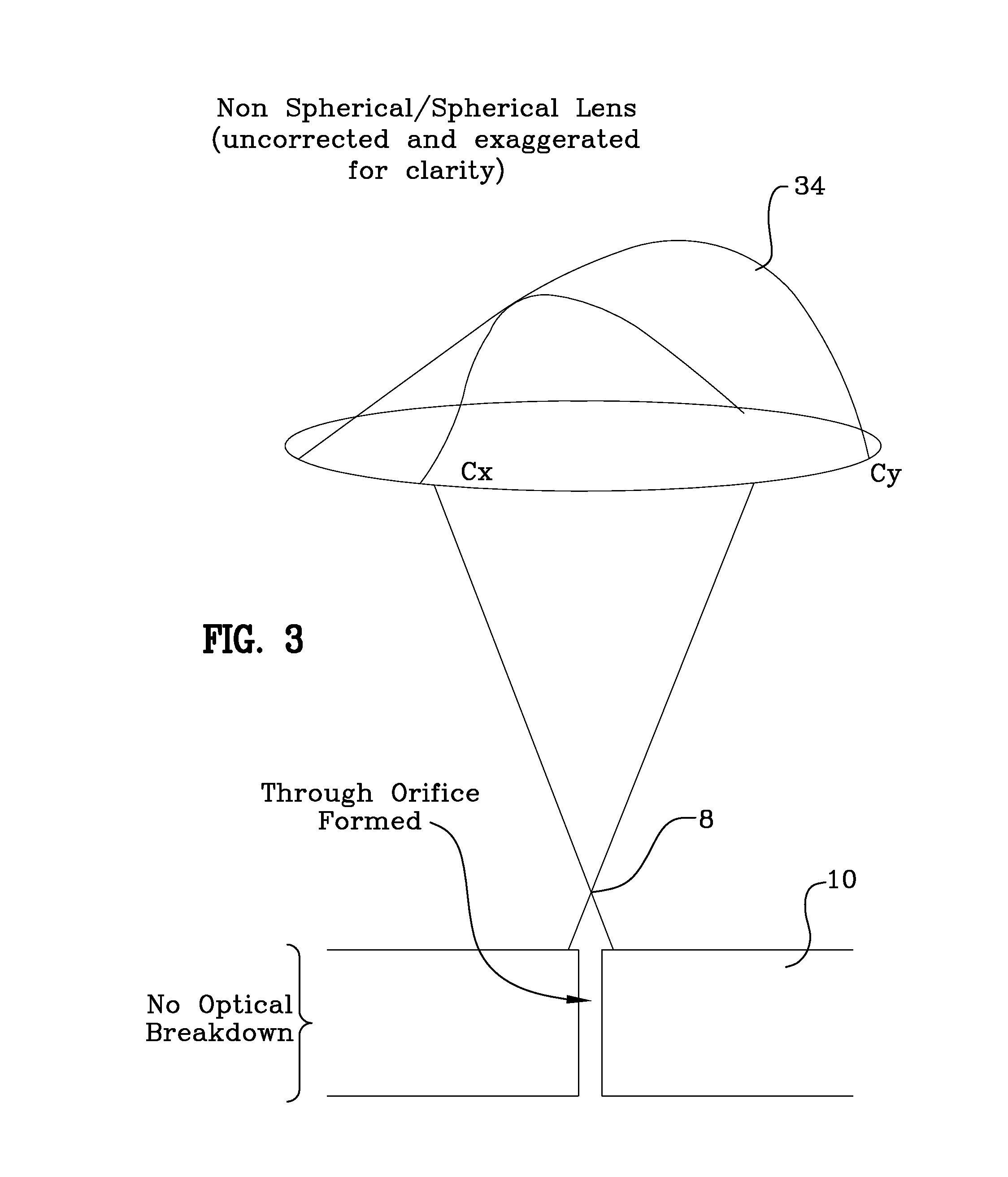
This patent describes a new technique to create very small cuts and orifices in transparent materials like silicon wafers. The technique uses burst ultrafast laser pulses that create a filament inside the material to create the orifice from the bottom up. The process results in smoother cuts, minimal damage to the material, and longer orifices that are consistent in size and shape. This technique offers a new, non-obvious method for creating these orifices and can be used in various industries such as semiconductor device fabrication.

Problems solved by technology

Since the most common lasers (such as YAG lasers) operate in the 1064 nm wavelength range, these lasers produce light that is partially absorbed by silicon and thus are unable to cleanly cut silicon by burst ultrafast pulsed laser induced filamentation techniques owing to the significant linear absorption of the laser pulses.
The prior art ablative methods of machining of Silicon with lasers having wavelengths less than 1.3 μm leave very rough cut surfaces, compromise the material with micro cracks, create surface ejecta mounds, create stress zones and are prone to causing large regions of collateral thermal damage.
While laser ablation processes can be dramatically improved by selecting lasers with wavelengths that are strongly absorbed by the medium (for example, deep UV excimer lasers or far-infrared CO2 laser), the above disadvantages cannot be eliminated due to the aggressive interactions inherent in this physical ablation process.
Further, the prior art laser ablation systems have low throughput times, and cannot attain as close a tolerance machining as can be achieved by the present method.

Method used


Image

  • Method and apparatus for laser processing of silicon by filamentation of burst ultrafast laser pulses
  • Method and apparatus for laser processing of silicon by filamentation of burst ultrafast laser pulses
  • Method and apparatus for laser processing of silicon by filamentation of burst ultrafast laser pulses

Examples


example 1

[0077]Referring to FIG. 10, a semiconductor wafer 77 that includes several devices 9 is covered with UV tape 78 on the device side. Sapphire 76 is layered on top 77B of the semiconductor wafer 77 as illustrated in FIG. 10. Sapphire is a Kerr medium. Unlike previously known methods of laser material processing, embodiments of the present invention utilize an optical configuration that focuses the incident beam 2 on the bottom or top of the substrate 77 but not within the substrate 77. Due to high peek power of the laser pulses which exceeds 5 MW (sufficient for self focusing in sapphire), the pulses immediately start self focusing on the Kerr medium 76. The nonlinear effects help focus the laser pulses of the laser beam below the diffraction limit and create filamentation in the sacrificial layer made of sapphire 76. The process creates combined white light generation and conical emission 75 just below the transparent silicon target 77.

[0078]The white light spectrum is partially abso...

example 2

[0122]Making thin layers of wafers from a Silcon ingot is challenging. Presently, ingots are sliced using a saw and a lot of material is wasted. A proton beam is used to cut very thin layers of wafers but the proton beam process is expensive and difficult to do in a manufacturing environment.

[0123]Recently, it has been proposed that using optical breakdown by tight focusing of the beam inside the target beneath the top surface a region of defect along the cut line can be created. But separating the thin layer is challenging since there is no first initial scribing location.

[0124]As shown in FIG. 12, it is possible to make a 2 mm long scribe 31 along the edge 90E of the ingot 90 which helps release the thin sheet 90S (wafer) from Silicon ingot 90. Again this can be done using an ultrafast burst laser running above 1.3 μm wavelength or using an OPG or applying Kerr layer on the wall of ingot and using typical wavelength to generate ultrafast burst white light laser as discussed in exa...

example 3

[0125]This example is hole / orifice drilling in silicon via burst of ultrafast laser pulses. If a single burst of ultrafast laser as explained in example 1 is used, it will generate orifices with micron or submicron sizes. Percussion drilling can be done by firing many burst of laser pulses in single location. Photoacoustic compression melts and pushes the material toward the wall of the orifice resulting in much wider holes. Holes / orifices of 20 μm diameter are achieved using 500 laser pulses from bursts of laser pulses running at a repetition rate of 50 kHz, and, each burst of laser pulses has 8 pulses running at 50 MHz. Using a sacrificial layer is useful for a wavelength shift but also helps in preventing orifice taper in the silicon. No taper occurs in the orifices / holes created in the silicon, however, taper occurs in the sacrificial layer. Debris from the sacrificial layer is deposited on the sacrificial layer and leaves the silicon surface clean. If holes / orifices are created...


PUM

PropertyMeasurementUnit
Lengthaaaaaaaaaa
Lengthaaaaaaaaaa
Lengthaaaaaaaaaa

Abstract

A method for laser processing of Silicon includes placing a Kerr material into engagement with the Silicon forming an interface therebetween. A laser beam is applied having at least one subpulse in a burst envelope operating at a first wavelength. The laser beam passes through a distributive lens focusing assembly and to the Kerr material. The first wavelength is modified to a plurality of second wavelengths, some of which are effective for processing Silicon. Photoacoustic compression processing is produced by the laser pulse energy by a portion of second wavelengths delivered through the interface and to the Silcon which initiates Kerr Effect self focusing which is propagated in the Silicon by additional energy input to the Silicon thus producing a filament within the Silicon.

Description

[0001]This patent application claims priority to and the benefit of U.S. provisional patent application Ser. No. 61 / 911,345 filed Dec. 3, 2013. U.S. provisional patent application Ser. No. 61 / 911,345 filed Dec. 3, 2013 is incorporated herein in its entirety by reference hereto.BACKGROUND OF THE INVENTION[0002]The present invention relates to a method and apparatus for laser processing of a semiconductor substrate, more specifically, to the high quality laser cutting of monocrystalline and polycrystalline silicon resulting in near-zero kerf cuts with low total roughness, through the use of a standard wavelength laser.[0003]Silicon is transparent to light having a wavelength greater than 1.3 μm. Since the most common lasers (such as YAG lasers) operate in the 1064 nm wavelength range, these lasers produce light that is partially absorbed by silicon and thus are unable to cleanly cut silicon by burst ultrafast pulsed laser induced filamentation techniques owing to the significant linea...

Claims


Application Information

Patent Timeline
IPC IPC(8): B23K26/00B23K26/40B23K26/36B23K26/06B23K26/08
CPCB23K26/009B23K26/0057B23K26/4075B23K26/08B23K26/367B23K26/0648B23K26/0617B23K26/364B23K26/40B23K26/53B23K2103/50Y10T225/12Y10T428/12389Y10T428/24612
Inventor HOSSEINI, S. ABBAS
Owner ROFIN SINAR TECH
Learn More