Method for forming spacers for a transistor gate

a transistor gate and spacer technology, applied in the field of field effect transistors, can solve the problems of limited selectivity of attack of the underlying silicon, difficult to obtain spacers, surface consumption of silicon,

Active Publication Date: 2015-06-11
COMMISSARIAT A LENERGIE ATOMIQUE ET AUX ENERGIES ALTERNATIVES
View PDF3 Cites 19 Cited by
  • Summary
  • Abstract
  • Description
  • Claims
  • Application Information

AI Technical Summary

Benefits of technology

[0027]To achieve this objective, one aspect of the present invention concerns a method for forming spacers of a gate of a field effect transistor, the gate being situated on top of an active layer made from a semiconductor material, the method comprising a step of forming a pr

Problems solved by technology

With the known solutions, the reduction is size of the transistors makes it very tricky to obtain spacers completely fulfilling their role of isolation and not causing any defects in the realization of the transistors from SOI substrates.
The layer of oxide formed on the silicon retards the etching of the silicon at the cost however of a surface transformation of the latter into oxide and therefore a surface consumption of silicon.
The drawback of this type of etching is that the selectivity of attack of this underlying silicon is however limited.
So-called “wet” etchings based on hydrofluoric acid (HF) or phosphoric acid (H3PO4) are also used, which have a much better selectivity, respectively, vis-à-vis silicon or its oxide (SiO2) but which do not however make it possible to control the profile of the spacers since the etching is essentially isotropic in this case.
Under these conditions the ion implantation 105 for forming the source and drain regions 110 that will follow is liable to be very detrimental to the remaining monocrystal

Method used


Image

  • Method for forming spacers for a transistor gate
  • Method for forming spacers for a transistor gate
  • Method for forming spacers for a transistor gate

Examples


Embodiment Construction

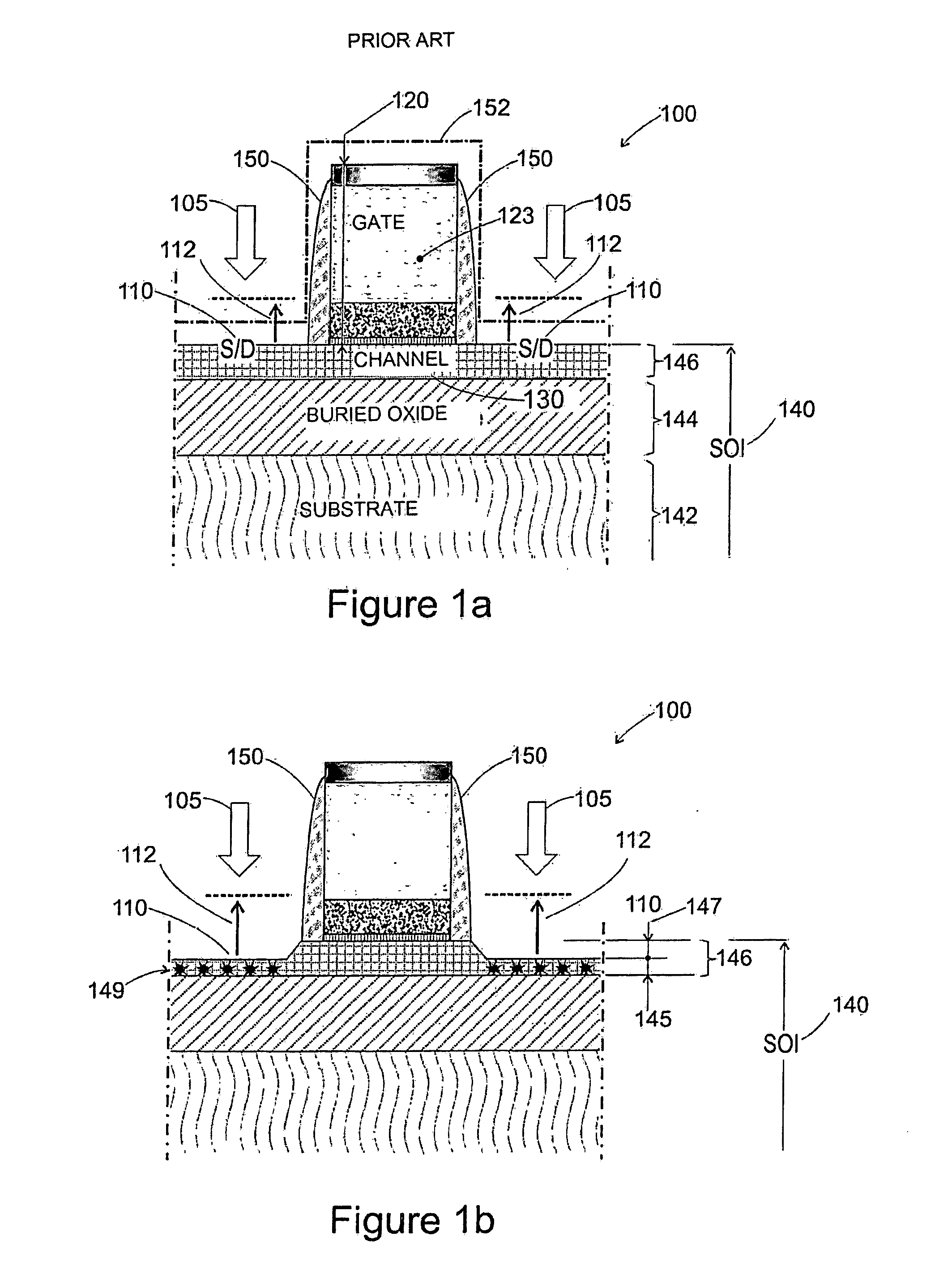
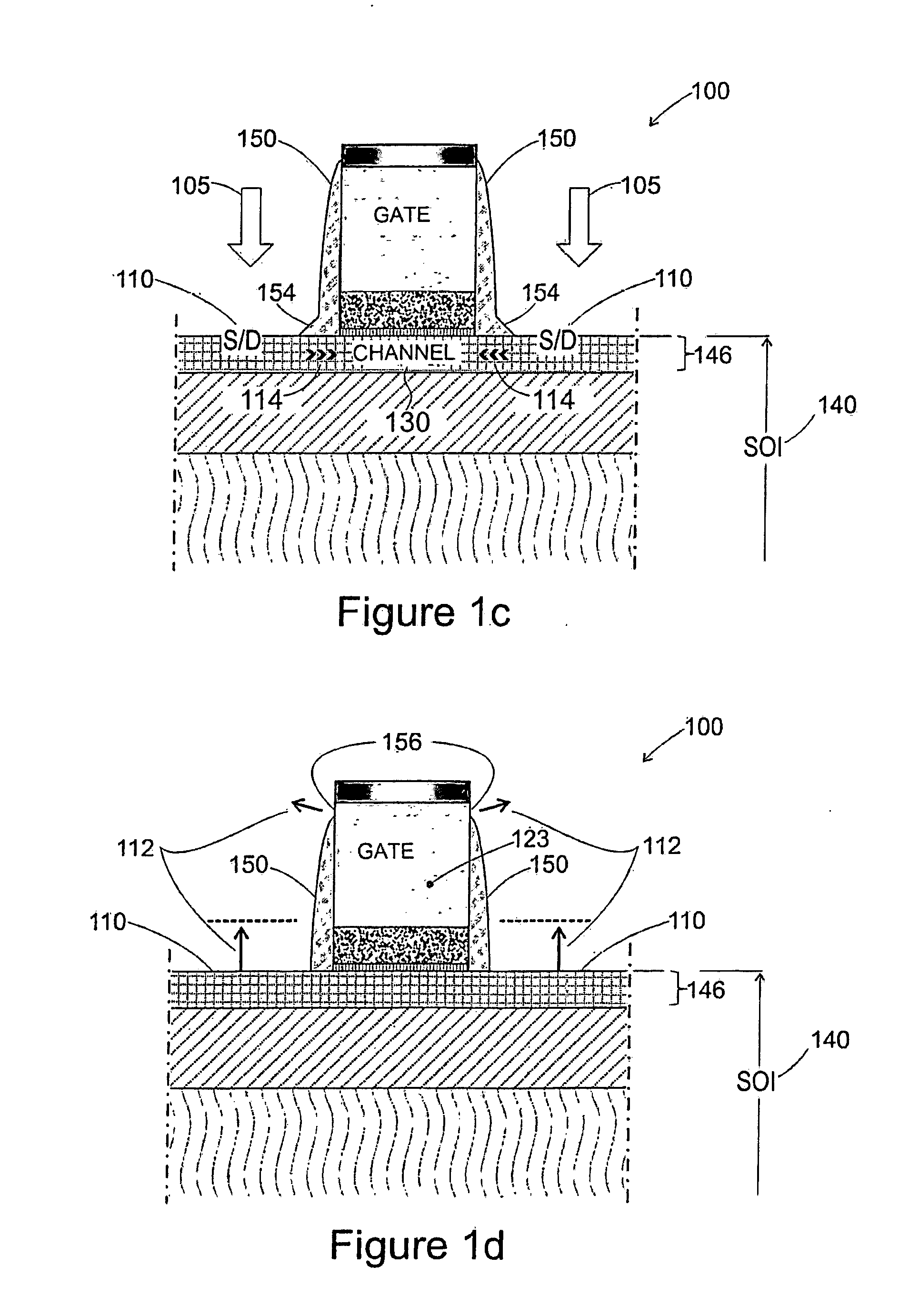
[0096]In the context of the present invention, the term “on”, “surmounts”, “cover” or “underlying” or the equivalent thereof do not necessarily mean “in contact with”. Thus for example the deposition of a first layer on a second layer does not necessarily mean that the two layers are directly in contact with each other but means that the first layer at least partially covers the second layer while being either directly in contact therewith or being separated from it by another layer or another element.

[0097]In the following description, the thicknesses are generally measured in directions perpendicular to the plane of the bottom face of the layer to be etched or of a substrate on which the bottom layer is disposed. Thus the thicknesses are generally taken in a vertical direction on the figures depicted. On the other hand the thickness of a layer covering a flank of a pattern is taken in a direction perpendicular to this flank.

[0098]The dielectric constants are for example measured b...


PUM


Abstract

A method for forming spacers of a transistor gate having an active layer surmounted by the gate, including forming a porous layer covering the gate and having a dielectric constant equal to or less than that of silicon oxide, forming a protective layer covering the porous layer and the gate, etching the protective layer anisotropically to preserve residual portions of the protective gate only at the flanks of the gate, forming a modified layer by penetration of ions within the porous layer anisotropically to modify the porous layer over its entire thickness above the gate and above the active layer and so as not to modify the entire thickness of the porous layer on the flanks of the gate, the latter being protected by protective spacers constituting porous spacers, and removing the modified layer by etching to leave the protective spacers in place.

Description

TECHNICAL FIELD OF THE INVENTION[0001]The present invention concerns in general field effect transistors (FET) used by the microelectronics industry and more particularly the realization of gate spacers of transistors of the metal-oxide-semiconductor (MOSFET) type mainly used for the production of all kinds of integrated circuit.PRIOR ART[0002]The incessant race for the reduction in size that characterizes the whole microelectronics industry could not have taken place except with the contribution of key innovations throughout the decades of development since the first integrated circuits were produced industrially in the nineteen sixties. A very important innovation that goes back to the nineteen seventies, and which is still used, consists of realizing MOSFET transistors by means of a technique in which the source and drain electrodes are auto-aligned on those of the gate and therefore do not require a photoetching operation for definition thereof. Combined with the use of gates ma...

Claims


Application Information

Patent Timeline
IPC IPC(8): H01L21/02H01L29/423
CPCH01L21/02126H01L21/02307H01L29/4232H01L21/02164H01L21/02274H01L21/823468H01L21/84H01L29/6653H01L29/6656H01L29/41783H01L29/66628H01L29/66772H01L29/66795H01L29/785
Inventor POSSEME, NICOLAS
Owner COMMISSARIAT A LENERGIE ATOMIQUE ET AUX ENERGIES ALTERNATIVES
Why Eureka
Try Eureka