

Production of mono-crystalline silicon
a mono-crystalline silicon and etching technology, applied in the field of crystalline silicon production, can solve the problems of reducing performance, exhibiting no consistency in the orientation of the crystalline structure, and the anisotropic etching process described above is not suitable for a multi-crystalline wafer, so as to improve the alignment of seed tiles and improve the performance of photovoltaic cells
- Summary
- Abstract
- Description
- Claims
- Application Information
AI Technical Summary
Benefits of technology
Problems solved by technology
Method used
Image

Examples
Embodiment Construction
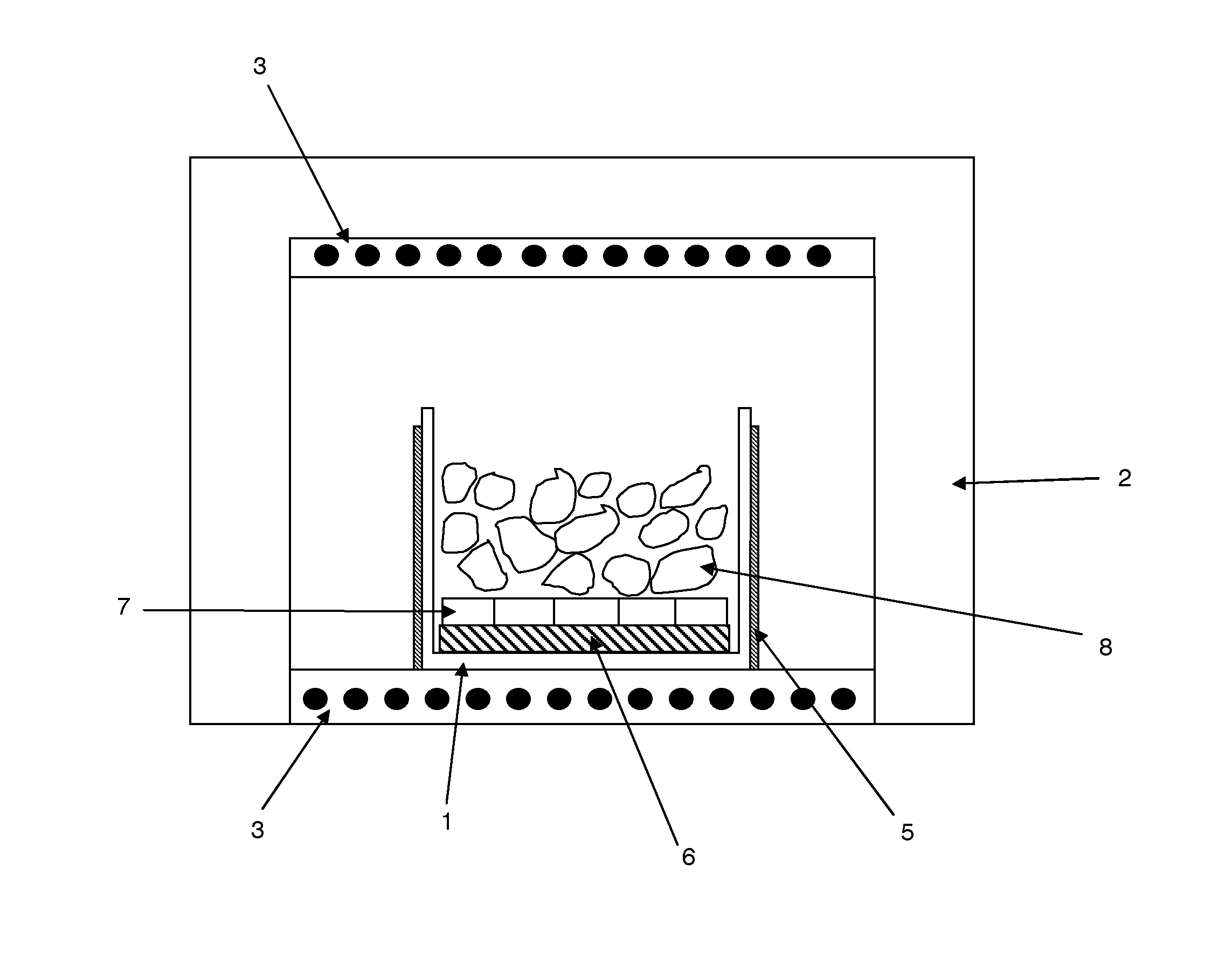
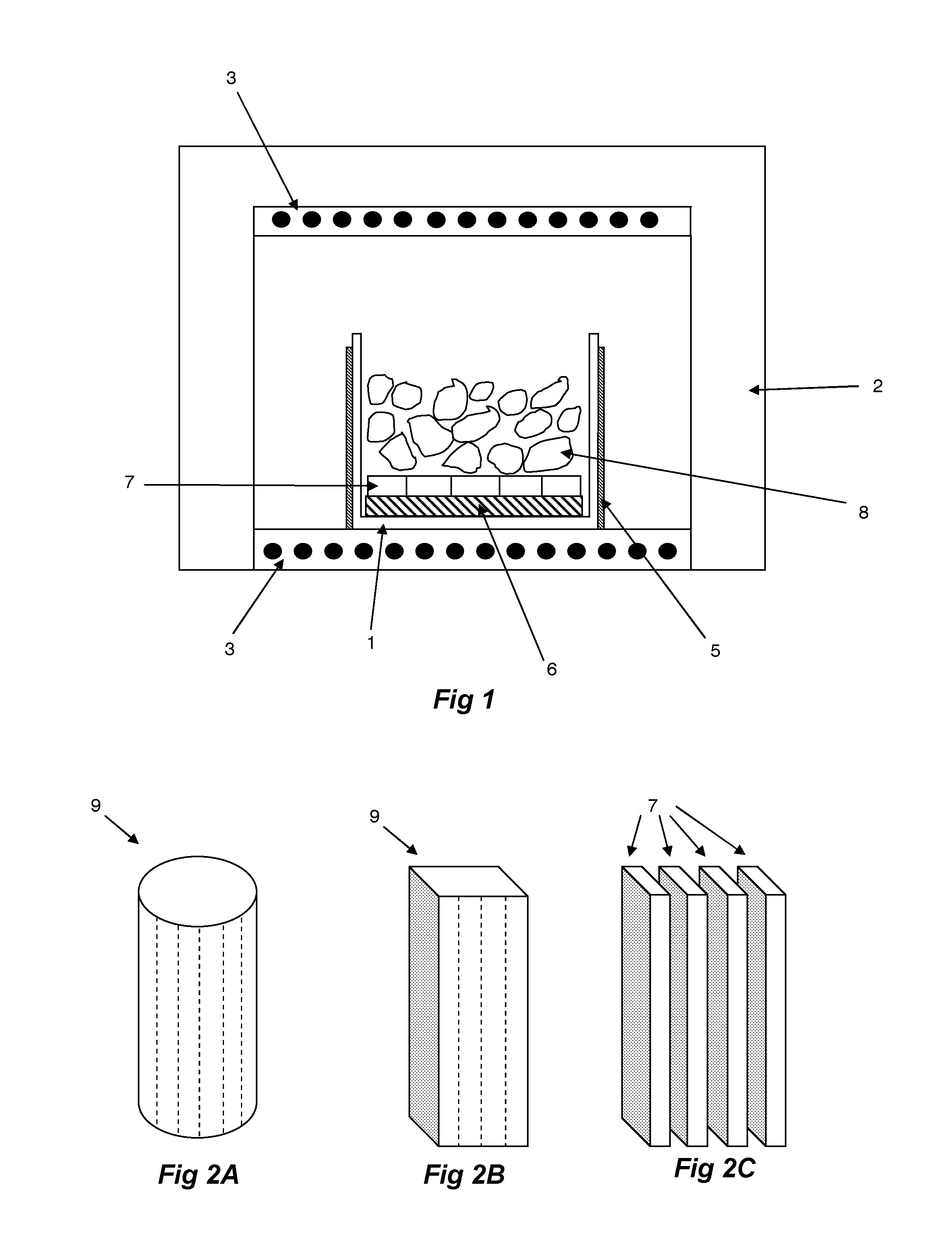
[0048]Referring to FIG. 1, there is provided a crucible 1 within a furnace hot zone 2. The walls of the furnace hot zone 2 may be formed of graphite or a similar material capable of withstanding high temperatures. In the preferred embodiment, the furnace hot zone 2 shown in FIG. 1 is one of a plurality of hot zones within a multi-ingot furnace. Each hot zone 2 may be substantially similar to that shown in FIG. 1.
[0049]The embodiment of FIG. 1 is suitable for use in a directional solidification process for the production of crystalline silicon. Such directional solidification processes include the Bridgman method and Vertical Gradient Freeze methods.
[0050]The crucible 1 is preferably formed of silica coated with a coating of silicon nitride. The coating assists in ensuring that solid silicon does not stick to the crucible walls during the crystallisation process and in the removal of crystalline silicon from the crucible after the crystallisation process has been carried out. In orde...
PUM
| Property | Measurement | Unit |
|---|---|---|
| Fraction | aaaaa | aaaaa |
| Angle | aaaaa | aaaaa |
| Angle | aaaaa | aaaaa |
Abstract
Description
Claims
Application Information