Semiconductor device

a technology of semiconductors and devices, applied in the field of semiconductor devices, can solve the problems of linear gain decline largely, increase in loss of high-frequency signals, etc., and achieve the effect of high gain and high outpu

Active Publication Date: 2015-08-20
PANASONIC INTELLECTUAL PROPERTY MANAGEMENT CO LTD
View PDF3 Cites 10 Cited by
  • Summary
  • Abstract
  • Description
  • Claims
  • Application Information

AI Technical Summary

Benefits of technology

[0011]An object of the present invention is to provide a semiconductor device operable with high output and high gain.
[0015]The high-pass matching circuit further includes the third wiring and the third capacitative element, so that the high-pass matching circuit having a desired characteristic can be designed without constraint on a thickness of the dielectric substrate and a wiring length of the first wiring. In other words, the high-pass matching circuit can be formed while the degree of design freedom of the semiconductor device is enhanced, and therefore the decrease in linear gain can be suppressed during the large signal matching.
[0017]Spread of a depletion layer generated in the diode can be adjusted by adjusting the bias voltage of the diode, and therefore a capacitance of the diode can be adjusted. The bias voltage is properly adjusted according to the operating frequency, which allows the characteristic of the high-pass matching circuit to be properly adjusted according to the operating frequency. As a result, even if the semiconductor device is operated in a wideband, the difference between the impedance during the large output operation and the impedance during the small output operation can be decreased to suppress the decrease in linear gain during the large signal matching.
[0025]In the semiconductor device of the present invention, the semiconductor device operable with high output and high gain can be made for the high-frequency use.

Problems solved by technology

However, in the conventional semiconductor device, there is a problem in that a linear gain decreases largely during high output or a problem in that a loss of a high-frequency signal increases to interrupt the high output and high gain.

Method used


Image

  • Semiconductor device
  • Semiconductor device
  • Semiconductor device

Examples


first exemplary embodiment

Third Modification of First Exemplary Embodiment

[0152]A semiconductor device according to a third modification of the first exemplary embodiment is substantially identical to the semiconductor device of the second modification, and the semiconductor device of the third modification differs from the semiconductor device of the second modification in that the semiconductor device of the third modification includes a capacitor between adjacent wiring patterns 501 and a bonding wire connecting wiring pattern 110 and the capacitor.

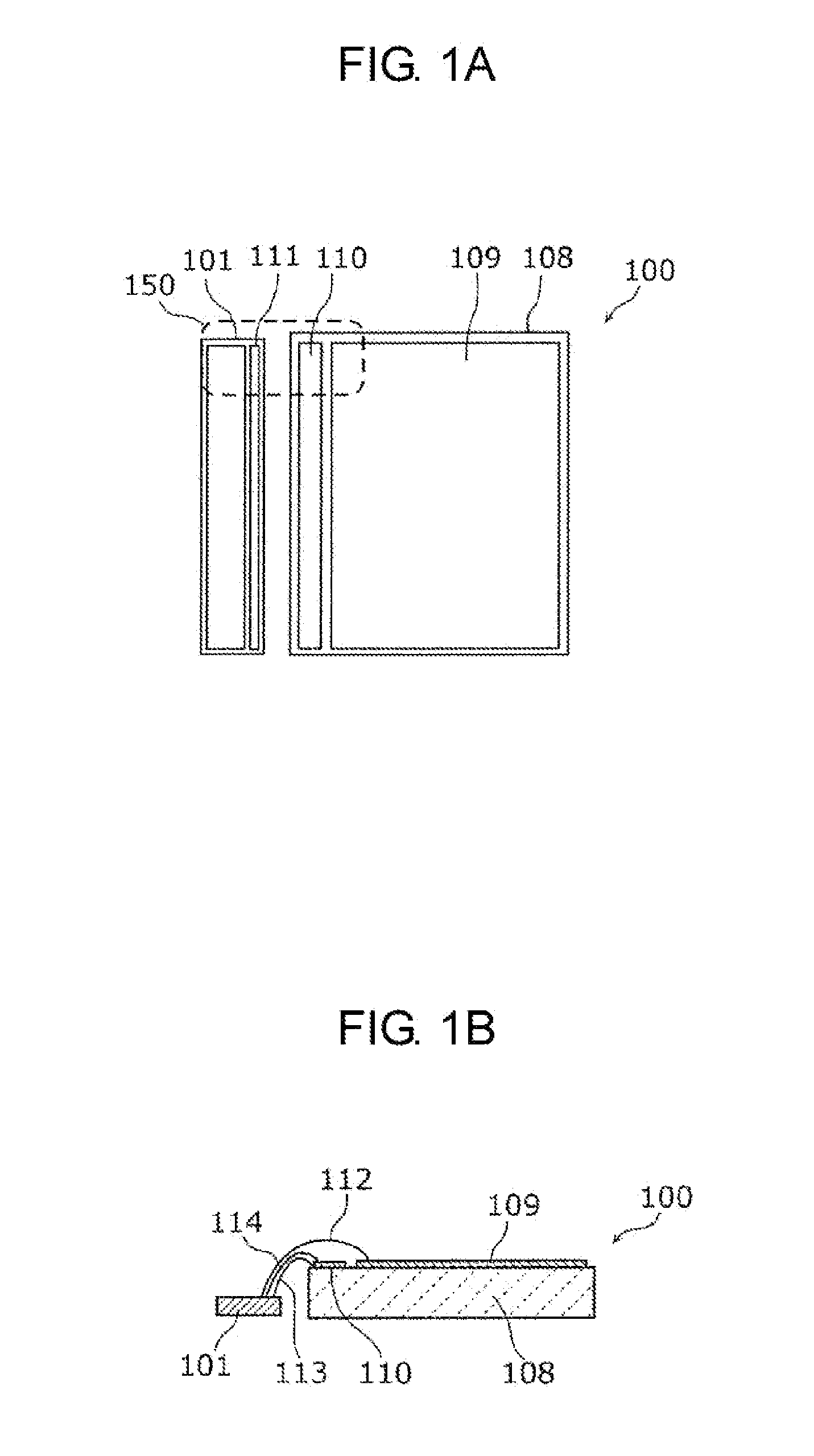
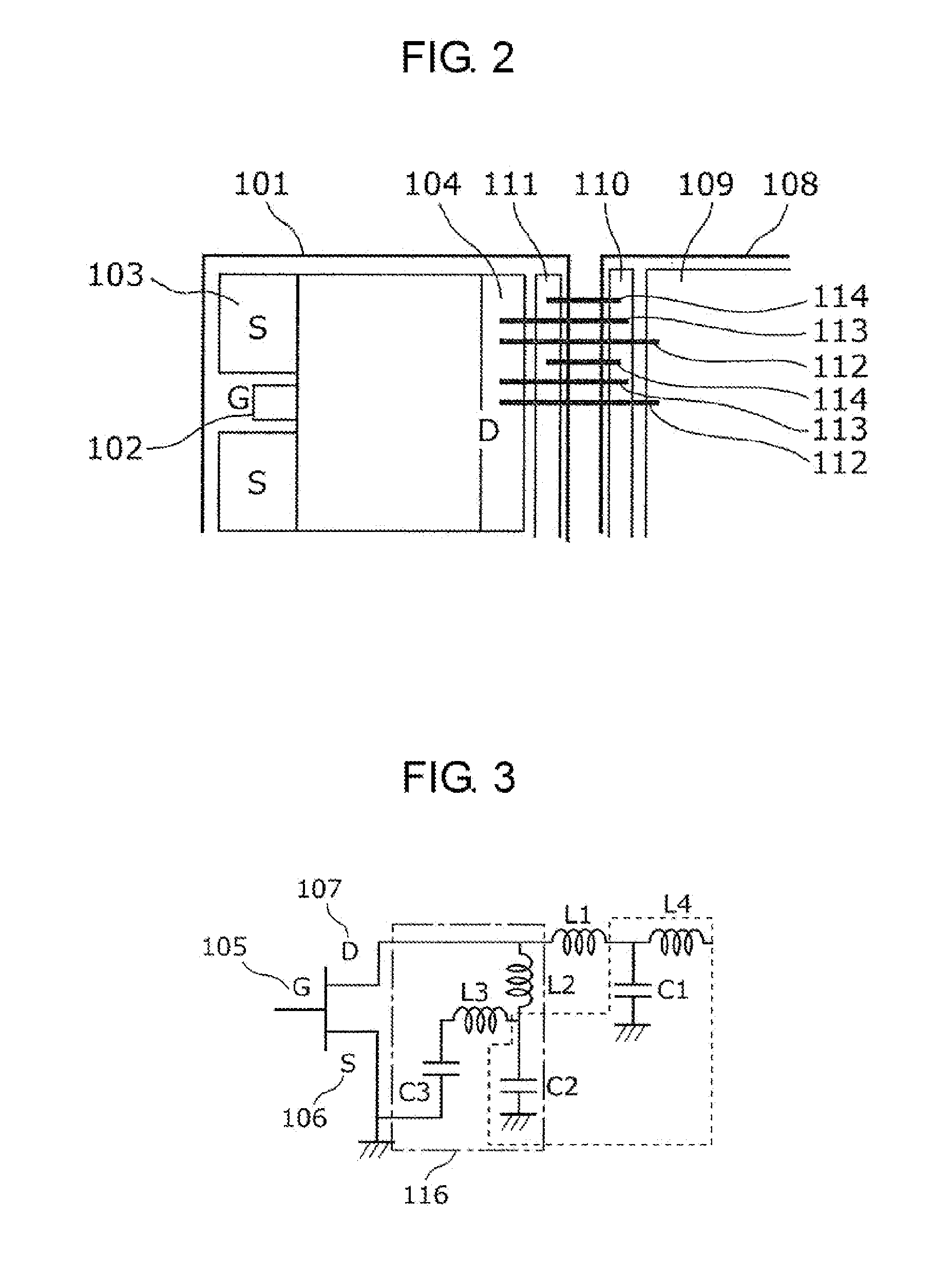
[0153]FIG. 8A is a plan view illustrating a configuration of the semiconductor device of the third modification, and FIG. 8B is an equivalent circuit diagram of the semiconductor device of the third modification.

[0154]Referring to FIG. 8A, drain pad 104 and wiring pattern 501 of semiconductor chip 101 are electrically connected to each other, wiring pattern 501 and wiring pattern 110 are electrically connected to each other by bonding wire 503, drain pad 104 an...

second exemplary embodiment

[0167]A semiconductor device according to a second exemplary embodiment differs from semiconductor device 100 of the first exemplary embodiment in that the semiconductor device of the second exemplary embodiment does not include the dielectric substrate and the bonding wire connecting the semiconductor chip and the dielectric substrate. That is, the semiconductor device of the second exemplary embodiment includes a capacitative element that is formed on a semiconductor chip and provided adjacent to the GaN HFET and stub wiring that is formed on the semiconductor chip to electrically connect one of electrodes of the capacitative element and an output terminal of the GaN HFET. The other electrode of the capacitative element is grounded, and the stub wiring and the capacitative element constitute the high-pass matching circuit that passes the signal having the operating frequency or more.

[0168]FIG. 9 is a plan view illustrating a configuration of the semiconductor device of the second ...

example 2-1

For Stub Wiring 205 Having a Length of 450 μm

[0192]FIG. 12 is a Smith chart illustrating the impedance during the small signal and the impedance during the large signal in semiconductor device 200 of Example 2-1 in which stub wiring 205 has a length of 450 μm and the semiconductor device of the comparative example that does not include the high-pass matching circuit.

[0193]FIG. 12 illustrates mismatch degrees of the impedance during the small signal and the impedance during the large signal in the semiconductor device of the comparative example and the semiconductor device of Example 2-1.

[0194]At this point, the impedance corresponds to the impedance of the unit cell having a gate width of 450 μm. That is, the impedance of a total gate width of 2.7 mm corresponds to the value in which the impedance of gate width 450 μm is parallelized.

[0195]Using the return loss (rl) introduced in the first exemplary embodiment, the return losses of the cases (1) and (2) are calculated and compared.

[...


PUM


Abstract

A semiconductor device includes a semiconductor chip, a dielectric substrate, and bonding wires. The dielectric substrate includes wiring patterns formed on a surface and a ground metal layer formed on a back side. The semiconductor chip includes an active element and a drain pad that is connected to an output end of the active element. Wiring pattern is formed at a position closer to the drain pad than wiring pattern, wiring pattern and the ground metal layer constitute a first capacitative element, and wiring pattern and the ground metal layer constitute a second capacitative element. The drain pad is connected to wiring pattern through bonding wire, and connected to wiring pattern through bonding wire. Bonding wire and the first capacitative element constitute a high-pass matching circuit.

Description

TECHNICAL FIELD[0001]The present invention relates to a semiconductor device.BACKGROUND ART[0002]In a microwave-band high-output power amplifier, there is a demand for high output and high gain to enhance the performance.[0003]Group III-V nitride semiconductors, namely, mixed crystal materials, such as gallium nitride (GaN), aluminum nitride (AlN), and indium nitride, the general formula of which is AlxGa1-x-yInyN (where 0≦x≦1 and 0≦y≦1), have physical features of a wide band gap and a direct transition band structure. Therefore, because of the features of high breakdown electric field and saturated electron velocity, application to electronic devices is also studied in addition to application to short-wavelength optical elements.[0004]Particularly, a Hetero-junction Field Effect Transistor (hereinafter, referred to as an HFET) in which 2-Dimensional Electron Gas (hereinafter, referred to as 2DEG) appearing at an interface between the AlxGa1-xN layer (where 0<x≦1) and the GaN lay...

Claims


Application Information

Patent Timeline
Patent Type & Authority Applications(United States)
IPC IPC(8): H03H7/38H01L49/02H01L27/06H01L29/778H01L29/861H03K3/01H01L23/528H01L29/20
CPCH03F3/195H03F3/60H03F1/565H03F3/193H03F2200/192H03F2200/195H03F2200/204H03F2200/207H03F2200/387H03F2200/391H01L23/66H01L2223/6611H01L2223/6655H01L2224/48091H01L2224/49175H01L2924/12032H01L2924/1305H01L2924/13091H01L2924/3011H01L2924/30111H01L2224/45144H01L28/60H01L2924/00014H01L2924/00H01L23/528H01L27/0629H01L29/2003H01L29/7787H01L29/861H03H7/38H03K3/01
Inventor NISHIJIMA, MASAAKI
Owner PANASONIC INTELLECTUAL PROPERTY MANAGEMENT CO LTD
Why Eureka
Try Eureka