Semiconductor device

a technology of semiconductor devices and reflux diodes, which is applied in the direction of semiconductor devices, diodes, electrical apparatus, etc., can solve the problems of increasing recovery loss, and achieve the effects of preventing leakage current from being increased, and increasing the unipolar current density of reflux diodes

Active Publication Date: 2015-08-20
MITSUBISHI ELECTRIC CORP
View PDF3 Cites 33 Cited by
  • Summary
  • Abstract
  • Description
  • Claims
  • Application Information

AI Technical Summary

Benefits of technology

[0010]In the semiconductor device according to the present invention, the impurity concentration of the first region provided in the lower part of the Schottky electrode is set to be higher than the first impurity concentration of the drift layer between the adjacent well regions. For this reason, a pn diode is operated with difficulty so that a unipolar current density of a reflux diode can be increased. Furthermore, the impurity concentration of the first region is set to be lower than the second impurity concentration of the well region. Therefore, a depletion layer is sufficiently extended in the lower part of the Schottky electrode in an OFF state. Consequently, an electric field to be applied to a Schottky barrier junction is relieved so that a leakage current can be prevented from being increased.
[0011]Moreover, in the semiconductor device according to the present invention, the impurity concentration of the first region provided in the lower part of the Schottky electrode is set to be higher than the first impurity concentration of the drift layer between the adjacent well regions. For this reason, the pn diode is operated with difficulty so that the unipolar current density of the reflux diode can be increased. Furthermore, the impurity concentration of the first conductivity type in the certain depth of the first region is set to be lower than the second impurity concentration of the well region in the same depth. Also in the case in which the second impurity concentration of the well region has a distribution in a depth direction, consequently, the depletion layer is sufficiently extended in the lower part of the Schottky electrode in the OFF state. Consequently, the electric field to be applied to the Schottky barrier junction is relieved so that the leakage current can be prevented from being increased.

Problems solved by technology

For example, in the case in which a pn diode is built in a structure of a semiconductor device such as an MOSFET, there is caused a problem in that a recovery loss is increased when the pn diode is operated in the use of a built-in Schottky barrier diode.

Method used


Image

  • Semiconductor device
  • Semiconductor device
  • Semiconductor device

Examples


first embodiment

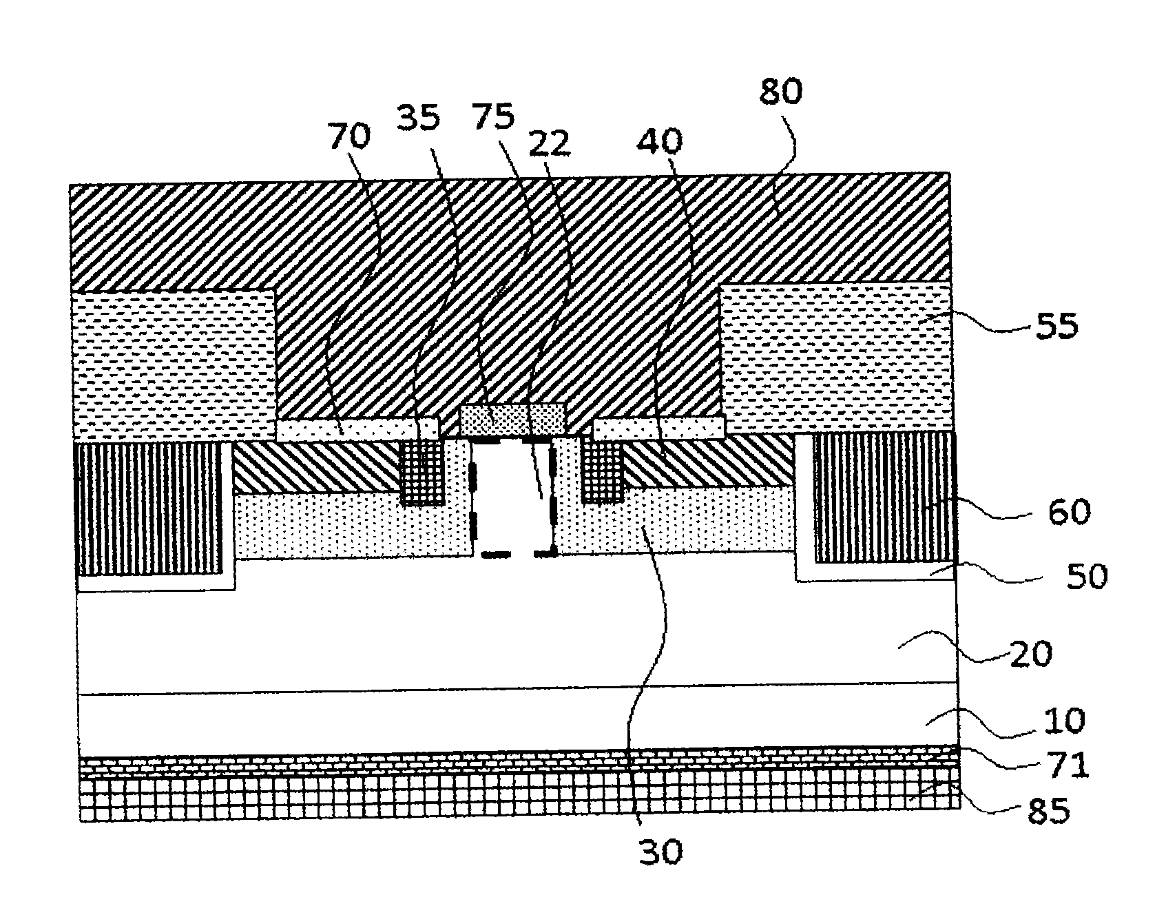
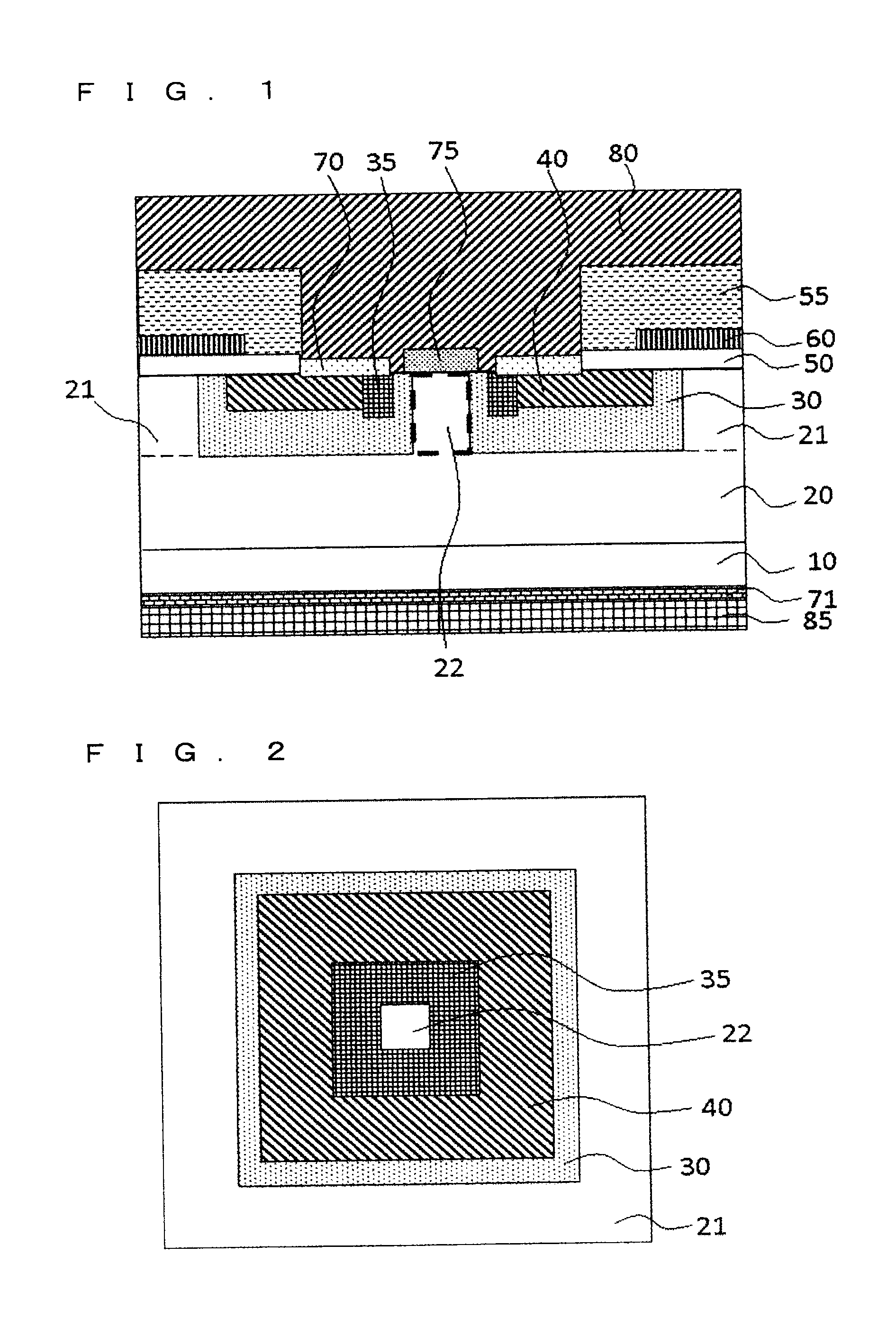
[0030]First of all, description will be given to a structure of a semiconductor device according to a first embodiment of the present invention. FIG. 1 is a sectional view showing the semiconductor device according to the first embodiment of the present invention and is a typical sectional view showing a unit cell of an MOSFET having a built-in SBD (Schottky Barrier Diode). FIG. 2 is a view showing a part of the semiconductor device according to the present invention as seen from above, and represents only a semiconductor region through transmission of an electrode, an insulating film and the like in FIG. 1. In the present embodiment, a silicon carbide (SiC) semiconductor device is taken as an example of the semiconductor device. Description will be given to an n-channel silicon carbide MOSFET in which a first conductivity type is set to be an n type and a second conductivity type is set to be a p type.

[0031]In FIGS. 1 and 2, a drift layer 20 constituted by n-type (first conductivit...

second embodiment

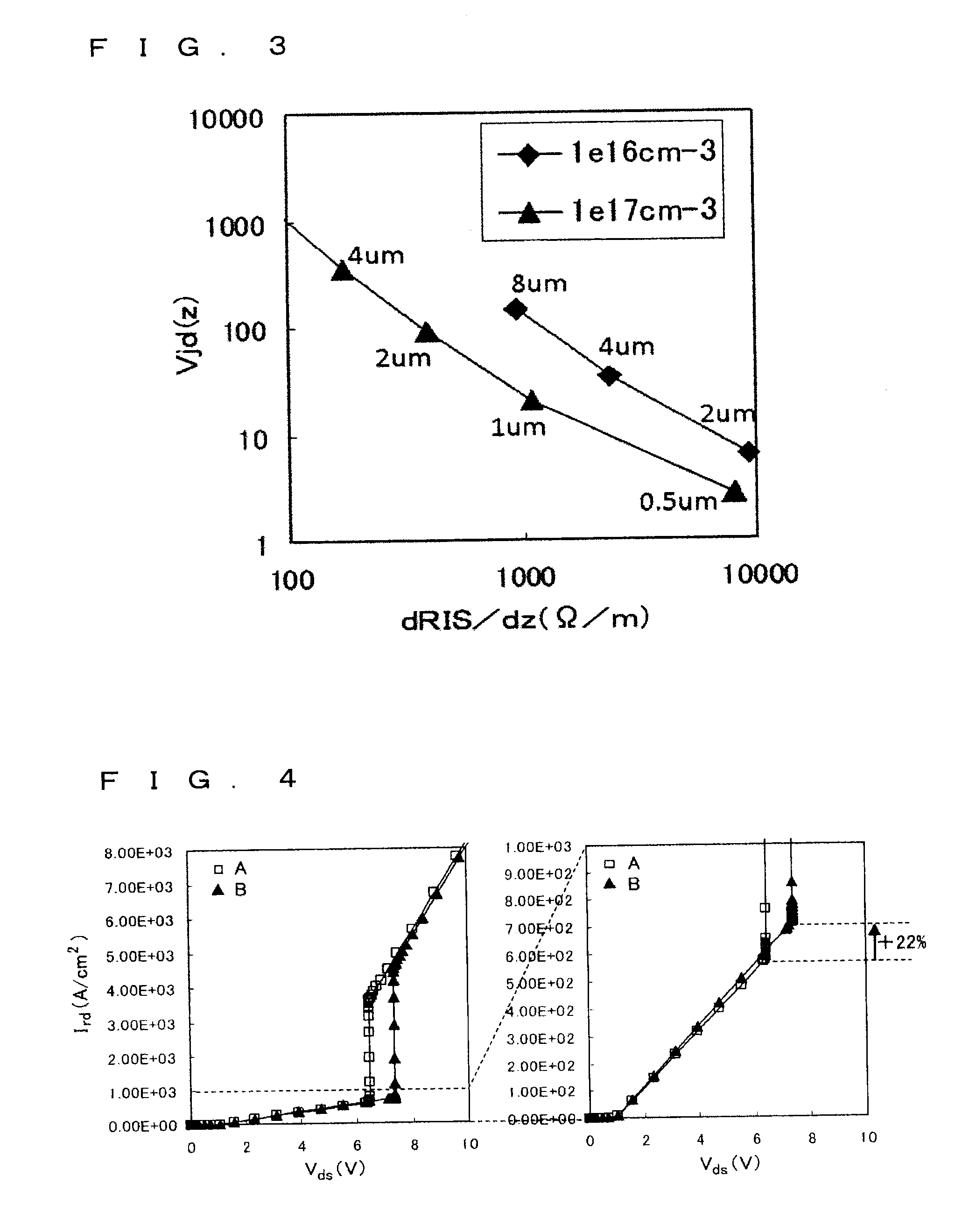
[0103]FIG. 5 is a chart showing an example of an impurity concentration profile of a first region in a first separation region 22 of a semiconductor device according to a second embodiment of the present invention. The second embodiment features that an n-type impurity concentration NNd in a first region is set to be higher in a deeper region than a shallow region from a surface. The others are the same as in the first embodiment.

[0104]In the present embodiment, the impurity concentration of the first region is higher than a first impurity concentration of a drift layer 20, and as shown in FIG. 5 which is an example of an impurity concentration profile, the profile has the impurity concentration which is attenuated toward an interface with a Schottky electrode 75. In FIG. 5, an axis of abscissa indicates a distance dSB from a Schottky barrier junction into the drift layer 20 and an axis of ordinate indicates the impurity concentration NNd in the first region.

[0105]In the present emb...

third embodiment

[0120]FIG. 10 is a sectional view showing a semiconductor device according to a third embodiment of the present invention. In FIG. 10, a region which is surrounded by a thick broken line and is equivalent to the first separation region 22 is a first region. In the third embodiment, furthermore, a region provided directly under a first separation region 22 and surrounded by a thick dotted line is referred to as a second region, and a region provided directly under a well region 30 and surrounded by a thick dashed-dotted line is referred to as a third region. The third embodiment features that n-type (first conductivity type) impurity concentrations of the second region provided in the lower part of the first region and the third region provided directly under the well region 30 as well as an impurity concentration of the first region of the first separation region 22 are increased with respect to a first impurity concentration of a drift layer 20. The others are the same as those in ...


PUM


Abstract

In a semiconductor device having a built-in Schottky barrier diode as a reflux diode, a maximum unipolar current is increased in a reflux state and a leakage current is reduced in an OFF state. A Schottky electrode is provided in at least a part of a surface between adjacent well regions of a second conductivity type disposed on a surface layer side of a drift layer of a first conductivity type, and an impurity concentration of a first conductivity type in a first region provided in a lower part of the Schottky electrode and provided between the adjacent well regions is set to be higher than a first impurity concentration of a first conductivity type in the drift layer and to be lower than a second impurity concentration of a second conductivity type in the well region.

Description

TECHNICAL FIELD[0001]The present invention relates to a semiconductor device.BACKGROUND ART[0002]In a semiconductor device such as an MOSFET (Metal-Oxide-Semiconductor Field-Effect-Transistor), it is possible to use a built-in diode as a reflux diode. There is proposed a method of building in and utilizing a Schottky barrier diode as a reflux diode (for example, see Patent Document 1).[0003]For example, in the case in which a pn diode is built in a structure of a semiconductor device such as an MOSFET, there is caused a problem in that a recovery loss is increased when the pn diode is operated in the use of a built-in Schottky barrier diode. For this reason, it is desirable that a unipolar current caused to flow by the Schottky barrier diode should be large in a state in which the pn diode is not operated (a bipolar operation). At this time, it is desirable to increase the unipolar current without enlarging a chip area, that is, to increase a unipolar current density, in order to re...

Claims


Application Information

Patent Timeline
Patent Type & Authority Applications(United States)
IPC IPC(8): H01L27/06H01L29/16H01L29/872
CPCH01L29/1608H01L29/66068H01L29/7806H01L29/7813H01L29/0696H01L29/0878H01L29/872H01L27/0629
Inventor HINO, SHIROMIURA, NARUHISAIMAIZUMI, MASAYUKI
Owner MITSUBISHI ELECTRIC CORP
Why Eureka
Try Eureka