Multilayer substrate and method for manufacturing the same

a multi-layer substrate and manufacturing method technology, applied in the direction of metal/alloy conductors, semiconductor/solid-state device details, transportation and packaging, etc., can solve the problems of over-resistance stress copper/ceramic interface fracture, etc., to improve the reliability of electronic packages

Inactive Publication Date: 2015-08-20
RSM ELECTRON POWER
View PDF11 Cites 8 Cited by
  • Summary
  • Abstract
  • Description
  • Claims
  • Application Information

AI Technical Summary

Benefits of technology

[0009]One objective of the present invention is to provide a slip layer substrate which can absorb/relieve the excess

Problems solved by technology

A common issue of the abovementioned structure where a multilayer metallized substrate with electronic devices populated is attached onto a metal heat spreader is the excessive residual stress caused by thermal expansion mismatch between the internal layers.
Temperature range of applications in automobile, military, and aerospace usually falls between −55° C. and 150° C. In some extreme cases, the application temperature can get as low as −65° C. and as high as 200° C. Exposure to such a wide temperature range can result in excessive thermal residual stress as high as several hundred mega Pascal in the multilayered structure, which can induce solder interface cohesive failure, copper/ceramic interface fracture, ceramic cohesive fracture, copper/solder adhesive failure, and even cracking of silicon electronic components.
As a result of these failures, the actual contact area between layers of the substrate is reduced, so that the elect

Method used


Image

  • Multilayer substrate and method for manufacturing the same
  • Multilayer substrate and method for manufacturing the same
  • Multilayer substrate and method for manufacturing the same

Examples


Embodiment Construction

[0033]For clarity of disclosure, and not by way of limitation, the detailed description of the invention is divided into the subsections that follow.

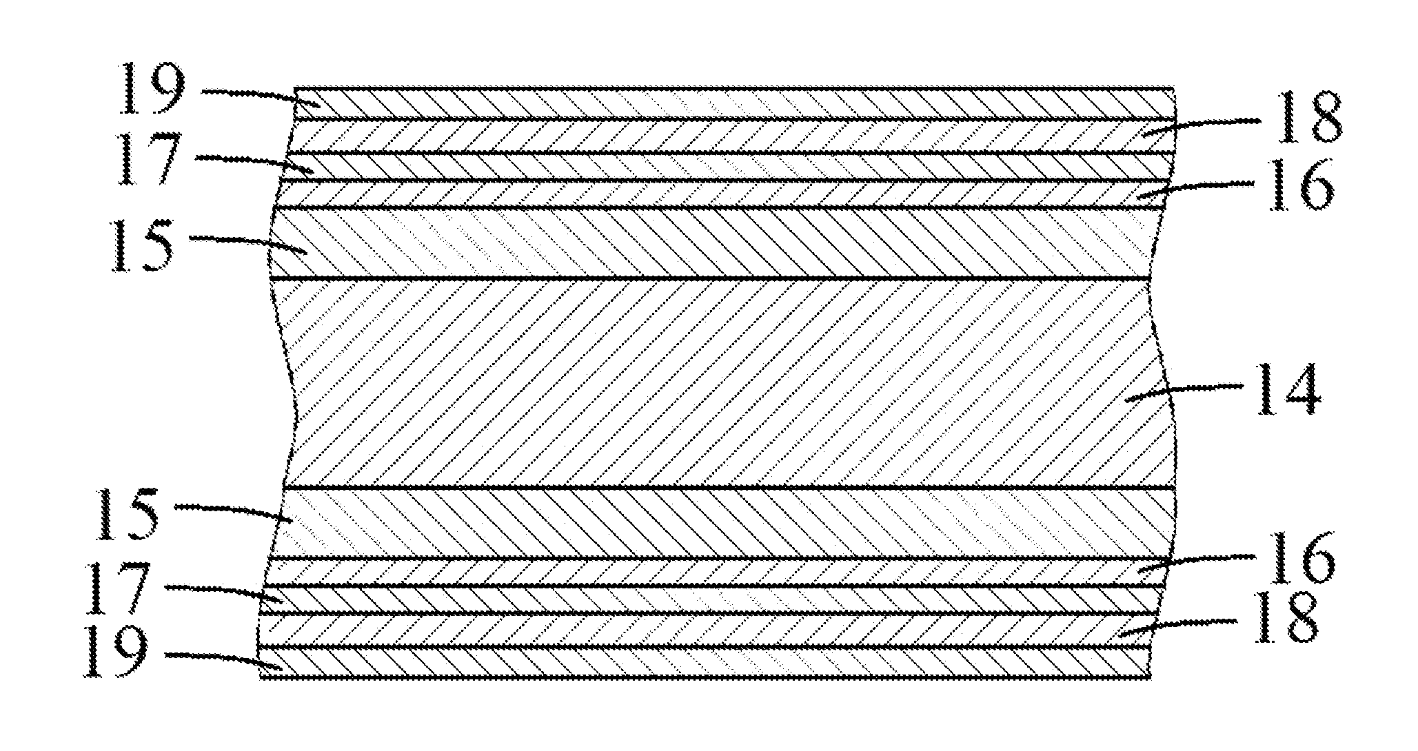
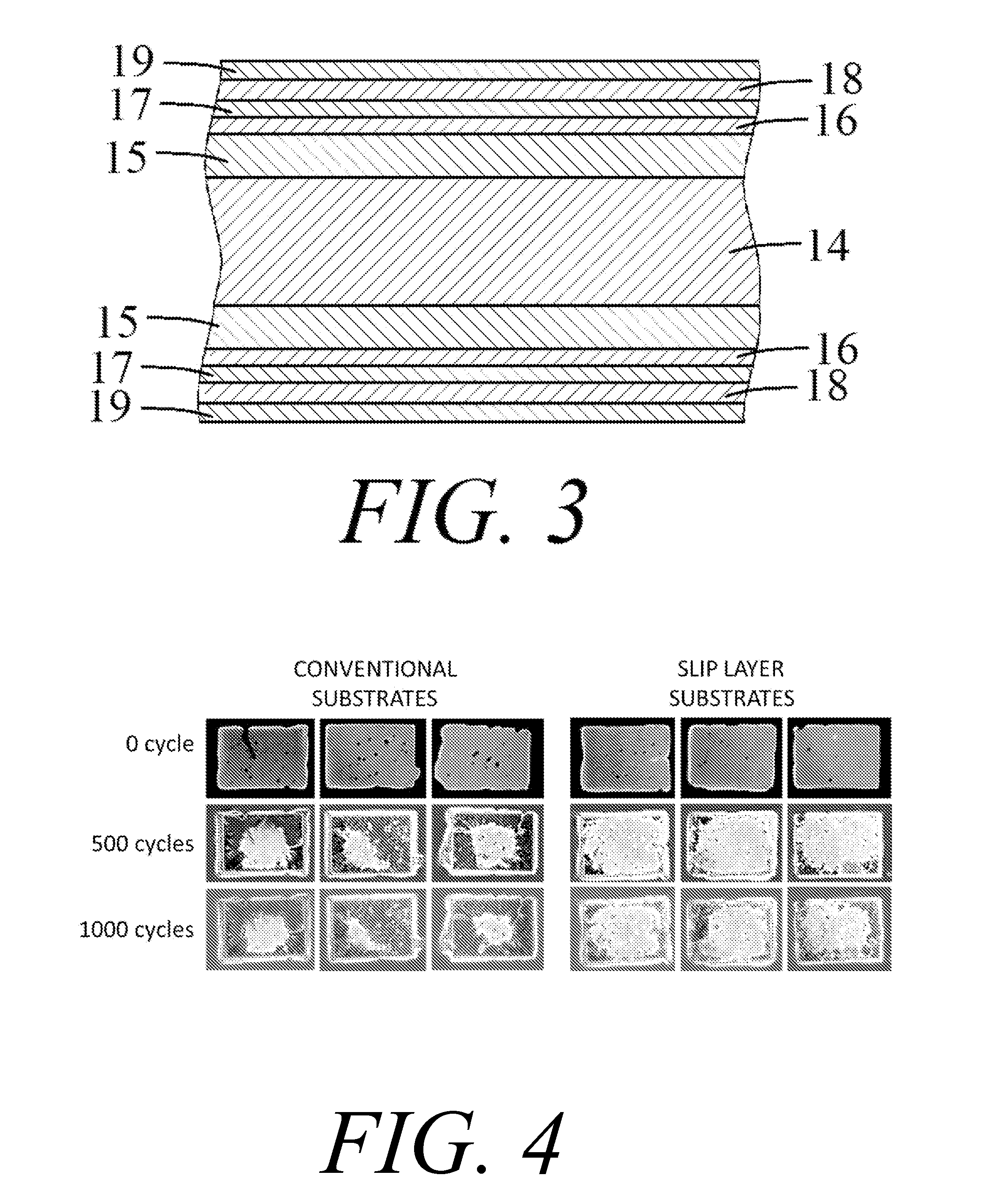
[0034]With reference to FIG. 2, this illustrates a schematic cross-section view of partial layers of the slip layer substrate of the present invention. A slip layer 17 is made of malleable and ductile materials, such as pure metals like gold, silver, aluminum or copper etc. and some malleable metal alloys and non-metals. Malleability is the property of a material where it can deform under compressive stress, while ductility refers to a material's ability to deform under tensile stress. For example, gold is the most malleable metal, and it can be beaten into extremely thin sheets. A gram of gold can be worked into a leaf covering 0.6 square meter, or into a wire 2.5 kilo meter in length. Both malleability and ductility are relative terms. In the circumstance of electronics packaging, material that sustains no less than 30% compression / el...


PUM


Abstract

The invention provides a slip layer substrate which can reduce the thermal residual stresses between components induced by their mismatch of thermal expansion, thus greatly improve the reliability of electronic packages. The slip layer substrate comprises: a base material; a first metallization layer formed on the base material; a first diffusion barrier layer formed on the first metallization layer; a slip layer formed on the first diffusion barrier layer; a second diffusion barrier layer formed on the slip layer; and a second metallization layer formed on the second diffusion barrier layer.

Description

NOTICE OF COPYRIGHT[0001]A portion of the disclosure of this patent document contains material which is subject to copyright protection. The copyright owner has no objection to any reproduction by anyone of the patent disclosure, as it appears in the United States Patent and Trademark Office patent files or records, but otherwise reserves all copyright rights whatsoever.BACKGROUND OF THE PRESENT INVENTION[0002]1. Field of Invention[0003]This invention relates to a substrate structure, and more particularly, to a multilayer substrate which reduces the residual stress induced by thermal expansion mismatch in electronic packages.[0004]2. Description of Related Arts[0005]Multilayer metallized substrates have been extensively used in electronic packages, such as DBC (direct bonded copper) substrate, AMB (active metal braze), DPC (direct plated copper), thick film plated up technology, and thin film technology. As an example, shown in FIG. 1, a typical DBC substrate consists of a ceramic ...

Claims


Application Information

Patent Timeline
IPC IPC(8): H05K1/03H01B13/00H01B1/02
CPCH05K3/244H05K2201/0341H01L23/3735H01L23/3736H01L2924/0002H05K2201/068Y10T428/12743Y10T428/1275Y10T428/12847Y10T428/12889Y10T428/12896Y10T428/1291H01L2924/00H01B1/02
Inventor AU, CHINGZHAO, MANHONGCONTE, ROBERT
Owner RSM ELECTRON POWER
Why Eureka
Try Eureka