
Optical element, illumination device, image display device, method of operating optical element

a technology of optical elements and illumination devices, applied in the direction of optical elements, thermoelectric devices, instruments, etc., can solve the problems of reducing the above-mentioned optical loss and restricting the image display device, and achieve the effect of high directivity and efficient light radiating

Inactive Publication Date: 2015-10-22
NEC CORP
View PDF46 Cites 3 Cited by
  • Summary
  • Abstract
  • Description
  • Claims
  • Application Information

AI Technical Summary

Benefits of technology

The present invention provides an optical element that can efficiently radiate light with high directivity at low etendue. This patent also includes an illumination device, an image display device, and an optical element operating method. The technical effect of this invention is achieving higher efficiency in lighting and image display.

Problems solved by technology

In addition, there is a restriction on the image display device due to an etendue determined by a product of an area of the light source device and an output angle thereof.
Accordingly, regarding light source devices including an optical element and an optical element to which light from the optical element is input, there has been an unsolved problem in that reduction of the above-mentioned optical loss is achieved by reducing an etendue of light output from the optical element.

Method used


Image

  • Optical element, illumination device, image display device, method of operating optical element
  • Optical element, illumination device, image display device, method of operating optical element
  • Optical element, illumination device, image display device, method of operating optical element

Examples


first exemplary embodiment

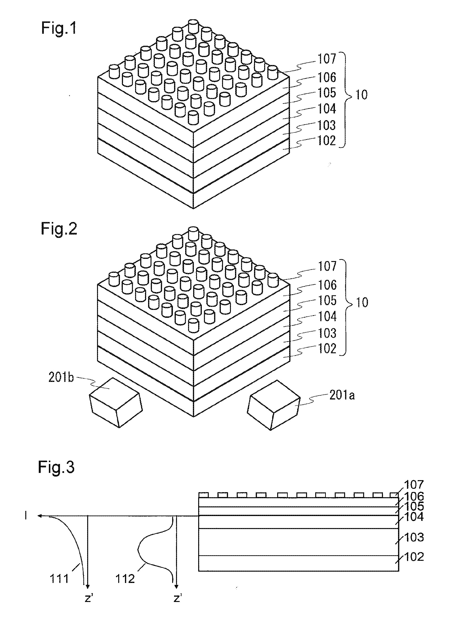
[0025]An optical element of the present exemplary embodiment is an example of an optical element including a dielectric layer. A perspective view of FIG. 1 depicts a structure of the optical element of the present exemplary embodiment.

[0026]As depicted in FIG. 1, an optical element 10 of the present exemplary embodiment includes a dielectric layer 102, a light emission layer 103 laminated on the dielectric layer 102, a dielectric layer 104 laminated on the light emission layer 103, a plasmon excitation layer 105 laminated on the dielectric layer 104, a dielectric layer 106 laminated on the plasmon excitation layer 105, and a wavenumber vector conversion layer (an output layer) 107 laminated on the dielectric layer 106.

[0027]The optical element 10 is configured such that a real part of an effective dielectric constant with respect to a surface plasmon in an excitation light incident side portion (which may be hereinafter referred to as “incident side portion”) is lower than a real pa...

second exemplary embodiment

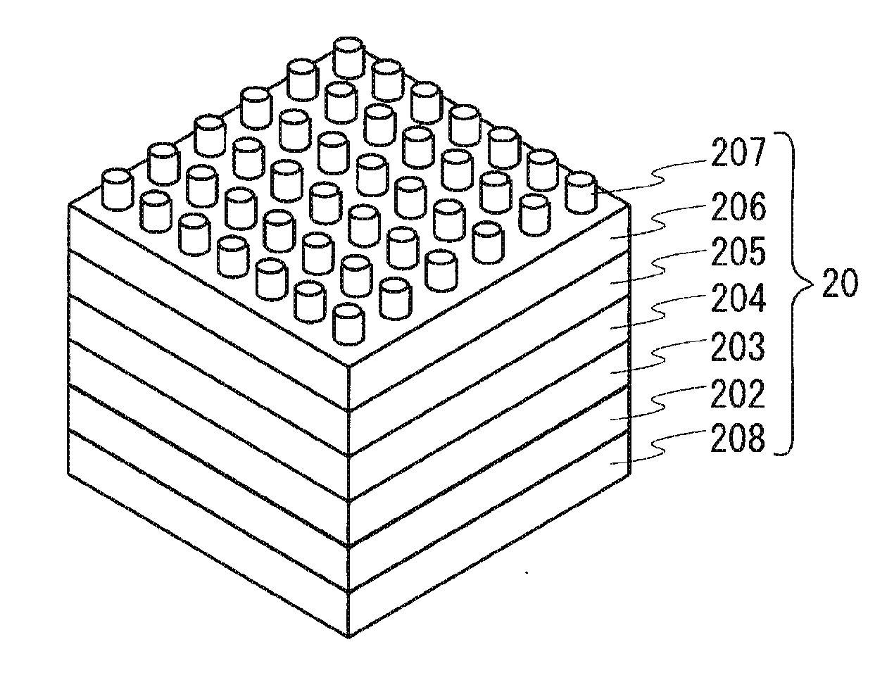
[0095]Next will be a description of another exemplary embodiment of the optical element of the present invention. A perspective view of FIG. 5 depicts a structure of a light emitting element of the present exemplary embodiment. The light emitting element of the present exemplary embodiment is different from that of the first exemplary embodiment in that it is a light emitting element configured so as to be operated by injection of current.

[0096]As depicted in FIG. 5, a light emitting element 20 of the present exemplary embodiment includes an anode 208, a hole (a positive hole) transport layer 202, a light emission layer 203 laminated on the hole transport layer 202, an electron transport layer 204 laminated on the light emission layer 203, a plasmon excitation layer 205 laminated on the electron transport layer 204, a dielectric layer 206 laminated on the plasmon excitation layer 205, and a wavenumber vector conversion layer (an output layer) 207 laminated on the dielectric layer 20...

third exemplary embodiment

[0108]An image display device of the present exemplary embodiment is an example of a three-panel projection display device (an LED projector). FIG. 6 depict a structure of the projector of the present exemplary embodiment. FIG. 6(a) is a schematic perspective view of the LED projector of the present exemplary embodiment, and FIG. 6(b) is a top view of the projector.

[0109]As depicted in FIG. 6, a projector 100 of the present exemplary embodiment includes, as main constituent elements, three light source devices 1r, 1g, and 1b using at least one of the optical element of the first exemplary embodiment or the light emitting element of the second exemplary embodiment, three liquid crystal panels 502r, 502g, and 502b, a color synthesis optical element 503, and a projection optical system 504. The light source device 1r and the liquid crystal panel 502r, the light source device 1g and the liquid crystal panel 502g, and light source device 1b and the liquid crystal panel 502b, respectively...


PUM


Abstract

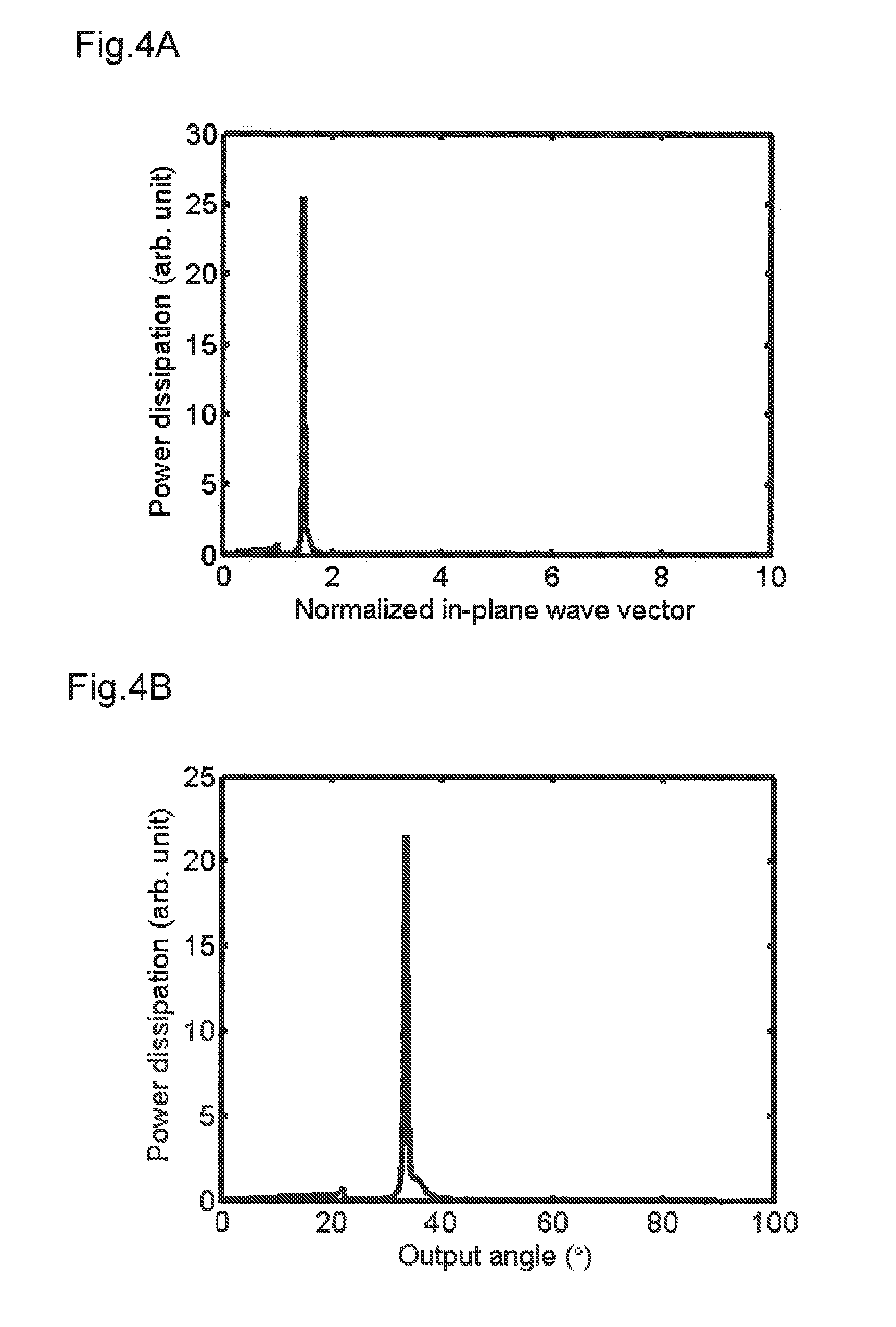
Provided is an optical element that highly efficiently radiates light with high directivity at low etendue. The optical element includes a light emission layer (103) generating an exciton to emit light, a plasmon excitation layer (105) having a higher plasma frequency than a light emission frequency of the light emission layer (103), an output layer (107) converting light or a surface plasmon generated on an upper surface of the plasmon excitation layer (105) into light with a predetermined output angle to output the light, and a dielectric layer (102). In the optical element, a real part of an effective dielectric constant with respect to the surface plasmon is higher in an upper side portion than the plasmon excitation layer (105) than in a lower side portion than the plasmon excitation layer (105); a dielectric constant with respect to the light emission frequency of the light emission layer (103) is higher in a lowest layer than in a layer adjacent to a lower side of the plasmon excitation layer (105); and assuming that a radiation angle of a surface plasmon-derived highly directional radiation from the plasmon excitation layer (105) to the output layer (107) side is θout,spp and a radiation angle of an optical waveguide fundamental mode-derived highly directional radiation is θout,light, an absolute value of a difference between the θout,spp and the θout,light is less than 10 degrees.

Description

TECHNICAL FIELD[0001]The present invention relates to an optical element, an illumination device, an image display device, and a method for operating an optical element.BACKGROUND ART[0002]An image display device such as a projector includes, for example, a light source device having an optical element, an illumination optical system to which light from the light source device is input, a light valve having a liquid crystal display panel to which light from the illumination optical system is input, and a projection optical system for projecting light from the light valve on a projection surface.[0003]The image display device is required to prevent optical loss as much as possible in an optical path from the light source device to the light valve in order to increase luminance of a projected image.[0004]In addition, there is a restriction on the image display device due to an etendue determined by a product of an area of the light source device and an output angle thereof. In other w...

Claims


Application Information

Patent Timeline
IPC IPC(8): G02B6/122H01L51/52G03B21/20H01L51/50
CPCG02B6/1226H01L51/5016H01L51/5056G02B2006/12123H01L51/5206G03B21/206H01L51/5072G03B21/2006H10K50/85H10K50/818H10K50/11H10K50/15H10K50/16H10K50/81H10K50/155H10K50/156H10K50/157H10K50/165H10K50/166H10K50/167H10K2101/10G03B21/204
Inventor NATSUMEDA, MASANAOIMAI, MASAOTOMINAGA, SHINSUZUKI, NAOFUMITOMIYAMA, MIZUHOOHNO, YUJI
Owner NEC CORP
Learn More