Silicon microsystems for high-throughput analysis of neural circuit activity, method and process for making the same

a silicon microsystem and neural circuit technology, applied in the field of silicon microsystems, can solve the problems of high cost of silicon microfabrication process, inability to fully understand the neural circuit, and inability to use commercial neural probes, so as to reduce the cost of production, less complex, and less invasive neural interface

Inactive Publication Date: 2015-11-26
RGT UNIV OF CALIFORNIA
View PDF3 Cites 20 Cited by
  • Summary
  • Abstract
  • Description
  • Claims
  • Application Information

AI Technical Summary

Benefits of technology

[0009]Provided herein is a fabrication process that is less complex, driving down the cost of production and making the prospect of disposable devices feasible for the first time. Also provided herein are the critical device dimensions offered by this manufacturing process are about 5-fold less than competing fabrication methods, allowing the development of narrower, hence less invasive neural interfaces.
[0010]Provided herein are probes of multi-electrode designs that readily allow recording with multiple electrodes simultaneously, and of two spatially distinct brain regions at the same time.

Problems solved by technology

However, monitoring network phenomena has been a major technological obstacle in systems neuroscience.
Furthermore, efforts to improve the therapeutic value of neuropsychopharmaceuticals must increasingly rely on an understanding of the underlying brain circuitry—such understanding remains incomplete.
Currently available commercial neural probes, typically based on silicon microfabrication processes are expensive ($100's to $1,000's per single chip) and do not meet the increasingly ambitious needs of the research community.
However, current tools fall short of providing a densely populated ‘activity map,’ which may offer a better understanding of the circuitry of cell assemblies in the brain.
Techniques such as electroencephalography (EEG) and functional magnetic resonance imaging (fMRI) provide coarse grained views on synchronized activity, but they do not afford much insight into the brain's circuitry at the level of single neurons.

Method used


Image

  • Silicon microsystems for high-throughput analysis of neural circuit activity, method and process for making the same
  • Silicon microsystems for high-throughput analysis of neural circuit activity, method and process for making the same
  • Silicon microsystems for high-throughput analysis of neural circuit activity, method and process for making the same

Examples


example 1

Exemplary Manufacturing of a Neural Probe

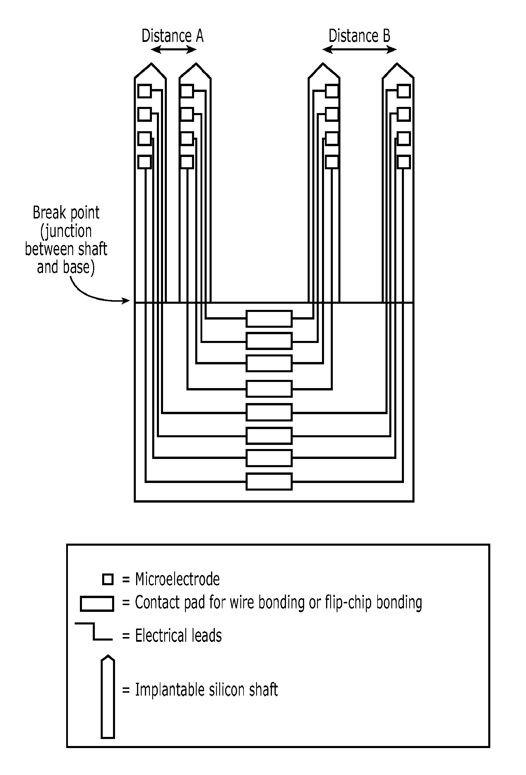
[0118]FIG. 5 depicts a neural probe with two arrays of mirrored contact pads for wire bonding or flip-chip bonding. To each array of contact pads is attached an ASIC.

[0119]In this example, the neural probe depicted in FIG. 5 was manufactured according to processes and methods described herein.

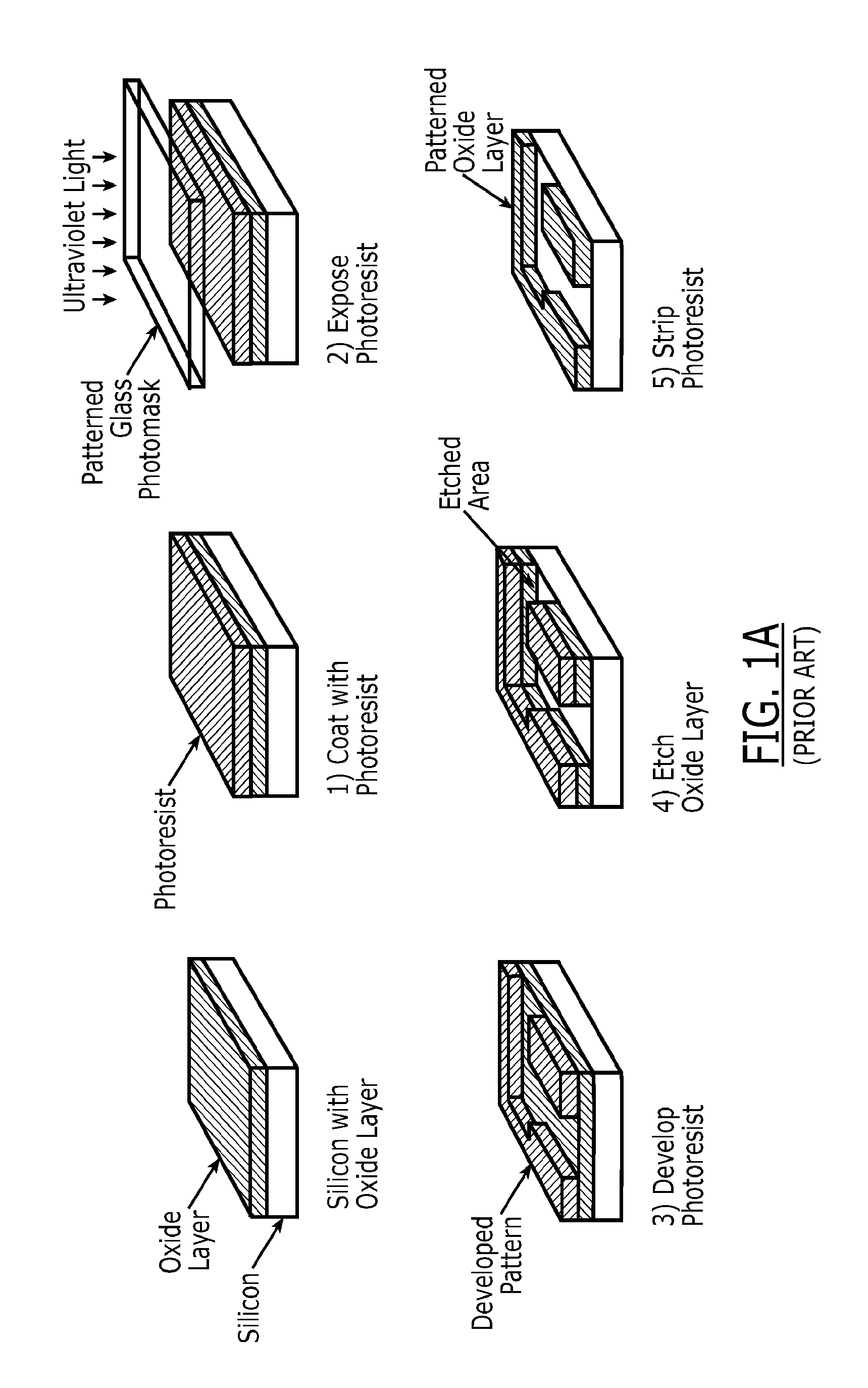
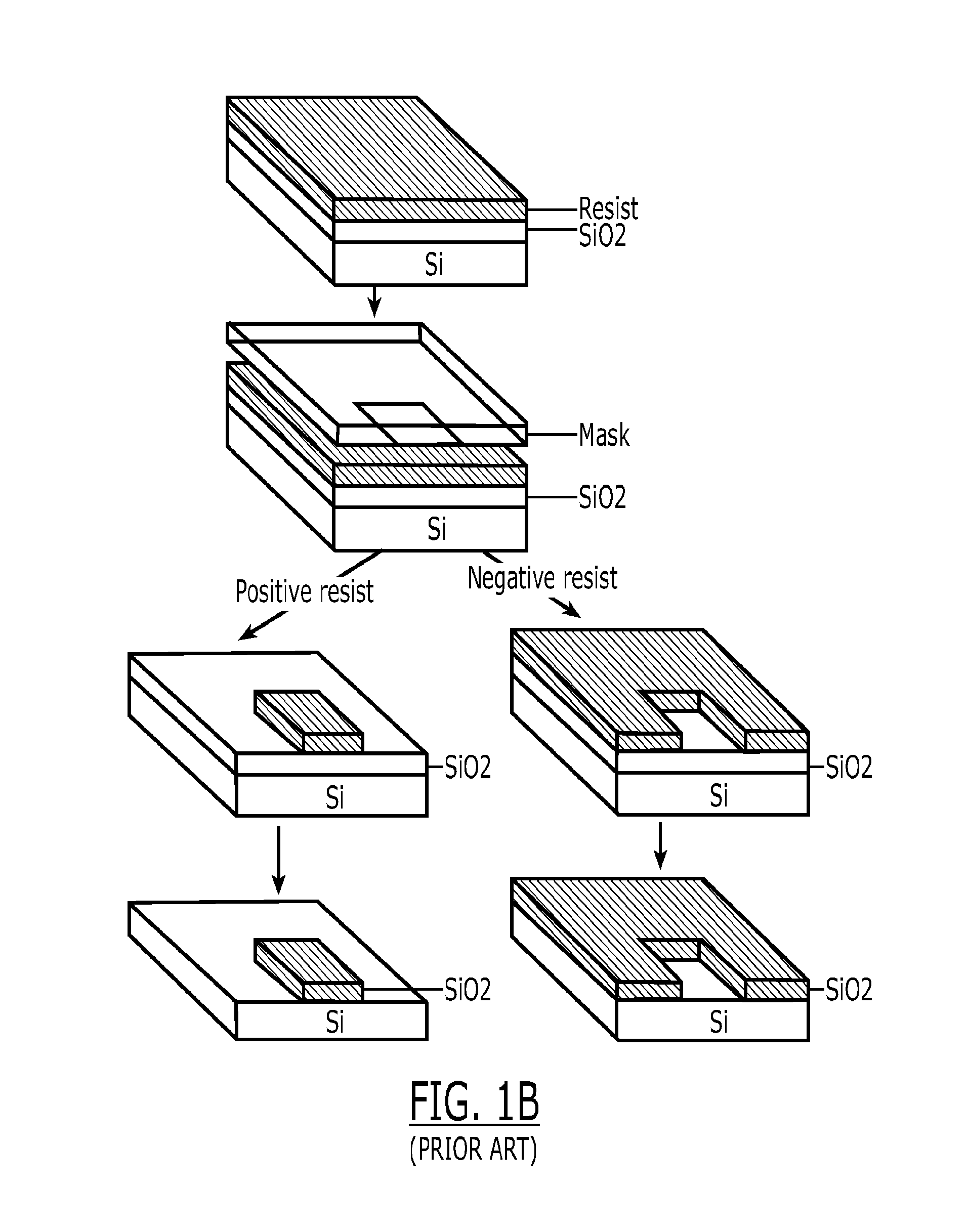
[0120]Fabrication took place on a 150 mm (6 inch) square silicon-on-oxide (SOI) substrate. A stepper mask aligner with a module bearing a square or rectangular reticle design was used to repeat a square or rectangular reticle pattern across the wafer. The reticle contained patterns for multiple variants of neural probes. The silicon device layer or substrate have thickness ranging from 10-50 microns.

[0121]The process steps were carried out as follows:[0122](i) depositing a layer of stress-free or low stress silicon nitride (e.g., at a thickness of 0.5 to 2 microns) on the top side of a substrate;[0123](ii) blanket-depositing Titanium / Gold / Platinum or a s...


PUM

PropertyMeasurementUnit
thicknessaaaaaaaaaa
thicknessaaaaaaaaaa
thicknessaaaaaaaaaa

Abstract

Provided herein are multi-electrode probe / microsystem designs that readily allow recording with multiple electrodes simultaneously, and of two spatially distinct brain regions at the same time. Also provide are methods and processes for manufacturing the probes.

Description

CROSS-REFERENCE TO RELATED APPLICATION[0001]This application claims priority to U.S. provisional patent application No. 61 / 732,259 filed on Nov. 30, 2012 and entitled “SILICON MICROSYSTEMS FOR HIGH-THROUGHPUT ANALYSIS OF NEURAL CIRCUIT ACTIVITY, METHOD AND PROCESS FOR MAKING THE SAME,” which is hereby incorporated by reference herein in its entirety.FIELD OF THE INVENTION[0002]The present invention relates to a novel process for manufacturing microsystems, which utilizes photolithography, etching and any other applicable methods and techniques. More specifically, the present invention relates to silicon microsystems containing implantable electrodes for measuring electrical signaling in the brain at the resolution of multiple single neurons, their designs, methods and processes for making the same.BACKGROUND OF THE INVENTION[0003]Large-scale studies of gene expression in the brain, such as the Allen Brain Atlas and the GENS AT project, have revolutionized the ability for identifying...

Claims


Application Information

Patent Timeline
Patent Type & Authority Applications(United States)
IPC IPC(8): A61B5/04A61B5/00
CPCA61B5/04001A61B5/4064Y10T29/49119A61B2562/125A61B5/6868A61B5/24
Inventor MASMANIDIS, SOTIRIS
Owner RGT UNIV OF CALIFORNIA
Why Eureka
Try Eureka