Emissivity controlled coatings for semiconductor chamber components

a technology of emissivity control and semiconductor chamber, which is applied in the field of thermal spraying coatings, can solve the problems of high number of particles, interference with precision processing steps, and contamination of semiconductor processing systems, and achieve the effects of reducing particle generation, improving thermal efficiency, and reducing interface corrosion and dielectric breakdown

Active Publication Date: 2015-12-31
FM INDS
View PDF6 Cites 21 Cited by
  • Summary
  • Abstract
  • Description
  • Claims
  • Application Information

AI Technical Summary

Benefits of technology

[0009]In addition to addressing the issues of plasma erosion prevention and reducing particle generation, the present invention also aims to improve thermal efficiency, an

Problems solved by technology

These substances, however, are typically quite corrosive to the semiconductor chamber components surrounding the work pieces, and the corrosion can cause the generation of particles within the chamber that contaminate the semiconductor processing system and interfere with the precision processing steps.
It should be noted, however, that once the densified skin coating is eroded or the top layer is cracked, the undercoating layers can be suddenly exposed, which would result in a sudden increase in plasma erosion and generation of a very high number of partic

Method used


Image

  • Emissivity controlled coatings for semiconductor chamber components
  • Emissivity controlled coatings for semiconductor chamber components
  • Emissivity controlled coatings for semiconductor chamber components

Examples


example 1

[0062]Test samples were made using a 6061T6 aluminum substrate. The substrates were roughened by grit-blasting to reach a surface roughness of about 200 μin Ra. The substrates were coated with 0.004 to 0.006 inch of emissivity controlled yttria coating (Y1.5O2.5). The DC plasma spray with shrouding mechanism was used according to the same process described above to deposit the coatings using a mixture of ionized gases containing argon, nitrogen and hydrogen in a ratio of 54:39:7%, respectively, as described above, without any substantial presence of oxygen.

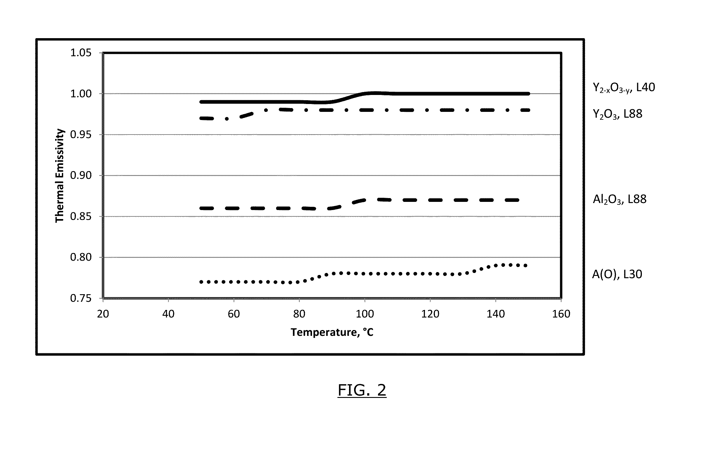
[0063]The color of the samples appeared black with L=40, a=−0.2 and b=−1.1, as measured by a spectrophotometer in accordance with the standard procedures established by the CIE (Commission Internationale de l'Eclairage, a.k.a., the International Commission on Illumination) for the L-a-b color space scale.

[0064]The hardness of the coatings was measured by a Vickers indentor according to standard procedures outlined in ASTM E384. Fo...

example 2

[0072]Test samples were made using 6061AL aluminum substrates that were roughened to 200 μin Ra by grit blasting, and then emissivity controlled co-phase (50 / 50 wt %) coatings of yttria (YO), having a composition of Y1.5O2.5, and yttria fully stabilized zirconia (YFSZ) having a composition of Y0.15Zr0.85O1.93, were applied by a DC plasma spray with shrouding mechanism according to the same process described above to deposit the coatings using a mixture of ionized gases containing argon, nitrogen and hydrogen in a ratio of 45:45:10%, respectively, without any substantial presence of oxygen.

[0073]The emissivity of the test samples were measured to be in a range of 0.98 to 0.99 over a temperature range of 50 to 160° C. The color of the samples, as measured with a spectrophotometer, appeared black with values of L=42, a=−0.5, b=−1.3. The coated samples were exposed to 5 wt % HCl for 24 hours. The area exposed to HCl did not show any signs of corrosion when examined under scanning electr...

example 3

[0076]Test samples were made using 6061 aluminum substrates. A wet corrosion barrier coating of 50 / 50 YFSZ / YO, having the composition of Y0.15Zr0.85O1.93 / Y1.5O2.5, was applied to a thickness of 0.004 inch by a DC plasma spray device with a shrouding mechanism using a mixture of ionized gases containing argon and hydrogen in a ratio of 90:10% without any substantial presence of oxygen described above. Then an emissivity controlled yttria coating (Y1.5O2.5) was applied to a thickness of 0.004 inches by a DC plasma spray device with a shrouding mechanism using the same mixture of ionized gases containing argon and hydrogen without any substantial presence of oxygen. The samples were then wiped with 5% HCl, ultrasonic cleaned in DI water, baked at 85° C., 110° C. and 220° C. These cycles of acid cleaning and thermal cycling were repeated 10 times, and then the bond strength of the samples was measured. It was found that the initial bond strength was 6000 psi and the retained bond streng...


PUM

PropertyMeasurementUnit
Thicknessaaaaaaaaaa
Concentrationaaaaaaaaaa
Electrical resistanceaaaaaaaaaa

Abstract

A component for a semiconductor processing chamber, the component including a substrate and a coating layer provided on a surface of the substrate, wherein the coating layer includes at least a first coating layer having a thermal emissivity of more than 0.98 to 1, having plasma resistance, and having a color value L in a range of 35 to 40 through a thickness direction thereof.

Description

FIELD OF THE INVENTION[0001]The present invention relates to thermal sprayed coatings for plasma chambers used in the etching or deposition processes of conductors or dielectric materials in the manufacture of semiconductor devices. In particular, the present invention relates to thermal emissivity controlled coatings for semiconductor processing chamber components.BACKGROUND OF THE INVENTION[0002]Semiconductor processing chambers are used for etching processes or the deposition of various materials inside a vacuum environment. These chambers have means for generating plasma to create energetic ions and a reactive chemistry that are used to perform the etching or deposition functions. These substances, however, are typically quite corrosive to the semiconductor chamber components surrounding the work pieces, and the corrosion can cause the generation of particles within the chamber that contaminate the semiconductor processing system and interfere with the precision processing steps...

Claims


Application Information

Patent Timeline
IPC IPC(8): C23C4/12C04B35/505C09K5/14C01F17/00C01F17/218
CPCC23C4/11C04B2235/3225C09K5/14C23C4/02C23C28/042C23C28/048C01F17/0018C01F17/0043C01P2006/32C04B35/505C04B35/486C04B2235/3244C23C4/134C04B41/009C04B35/111C04B35/52C04B35/565C04B35/581C01F17/218C04B35/62222C04B2235/3246C01F17/32
Inventor NAIM, MAHMOODHAMMERICH, DAVID
Owner FM INDS
Why Eureka
Try Eureka