

Copper particulate dispersion, conductive film forming method, and circuit board
a technology of conductive film and copper particulate, which is applied in the direction of conductive pattern formation, electrically-conductive paint, and conductors, etc., can solve the problems of insufficient photo-sintering, failure to form a conductive film with low electric resistance, and insufficient photo-sintering, etc., and achieves low electric resistance and easy formation
- Summary
- Abstract
- Description
- Claims
- Application Information
AI Technical Summary
Benefits of technology
Problems solved by technology
Method used
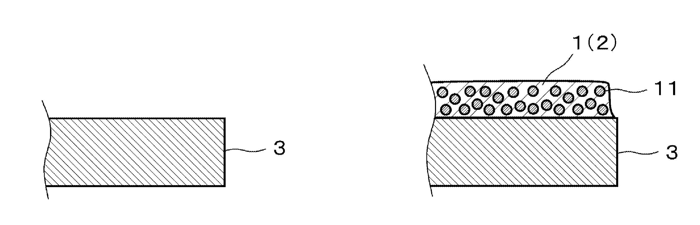
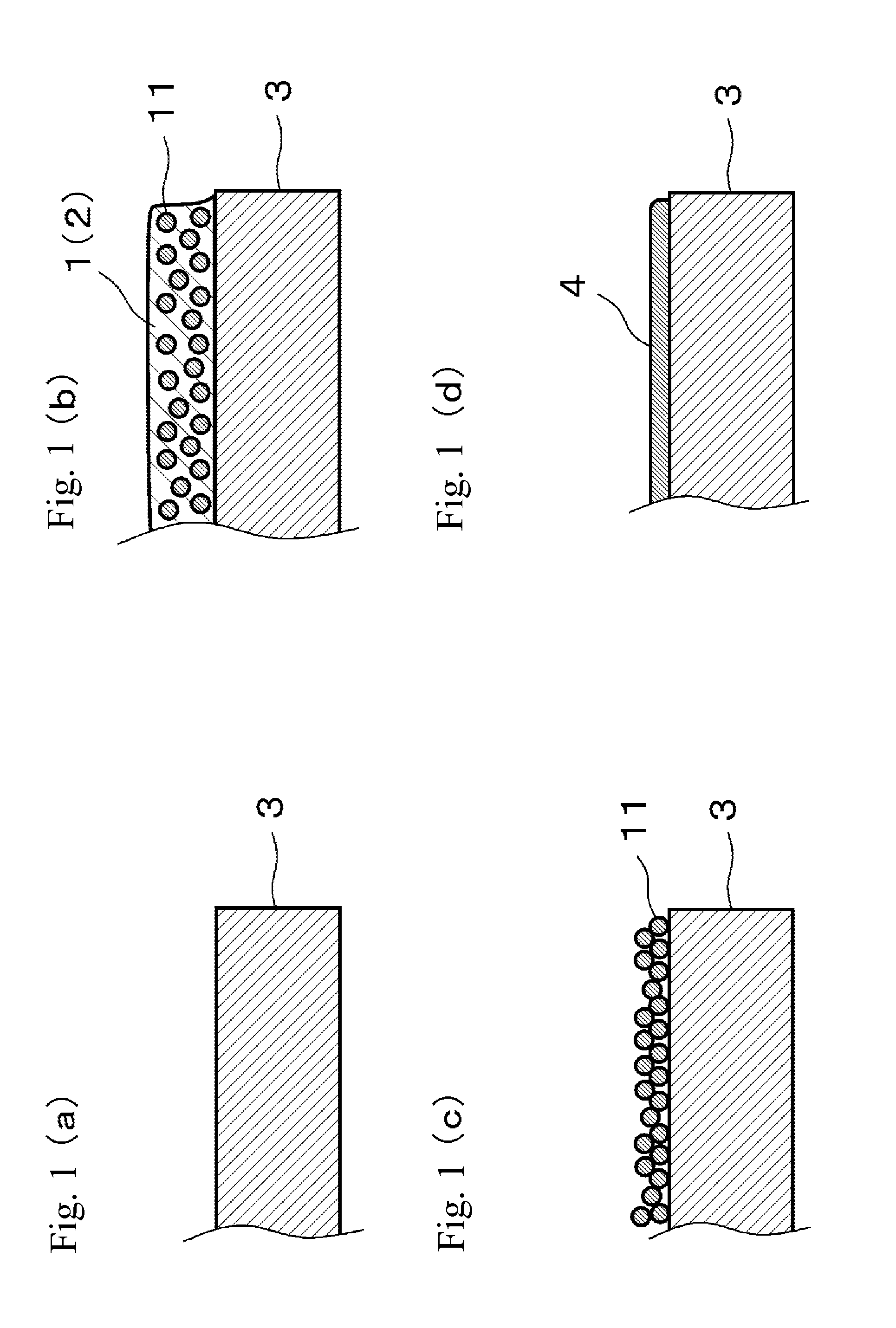
Image

Examples
example 1
[0037]A copper particulate dispersion in which a dispersant was added to disperse copper particulates in a dispersion vehicle was prepared. The dispersion vehicle was alcohol (diethylene glycol). This dispersion vehicle also served as a sintering promoter in this Example. The dispersant was phosphate ester (trade name: “DISPERBYK (registered trademark)-102,” available from BYK-Chemie). The concentration of the dispersant was 2 mass % with respect to the copper particulate dispersion. The copper particulates used had a mean particle size of 50 nm, and the concentration of the copper particulates was 40 mass %. A glass slide was used as a substrate.
[0038]The copper particulate dispersion was applied to the substrate by spin-coating to form a coating with a thickness of 1 μm. The color of the coating was black. The coating was irradiated with light, without drying. The light irradiation energy was 14 J / cm2.
[0039]The appearance of the coating was changed to the appearance of metal coppe...
example 2
[0040]The dispersion vehicle used was alcohol (diethylene glycol monoethyl ether) different from that of Example 1. This dispersion vehicle also served as a sintering promoter in this Example. The dispersant used was phosphate ester (trade name: “DISPERBYK (registered trademark)-111,” available from BYK-Chemie) different from that of Example 1. The other conditions were the same as those of Example 1. The appearance of the coating was changed to the appearance of metal copper by light irradiation, and a conductive film was formed on the substrate. The sheet resistance of the formed conductive film was 500 mΩ / sq.
example 3
[0041]A copper particulate dispersion was prepared using copper particulates having a mean particle size of 70 nm. Then, phosphate ester (trade name: “DISPERBYK (registered trademark)-111,” available from BYK-Chemie) was added as a sintering promoter to the copper particulate dispersion. This sintering promoter also served as a dispersant. The concentration of the sintering promoter was 10 mass % with respect to the copper particulate dispersion. A glass substrate (trade name “EAGLE XG (registered trademark),” available from Corning) was used as a substrate. The other conditions were the same as those of Example 2. A coating comprising the copper particulate dispersion was formed on the substrate. After the coating was dried, the coating was irradiated with light. The light irradiation energy was 11 J / cm2. The appearance of the coating was changed to the appearance of metal copper by light irradiation, and a conductive film was formed on the substrate. The sheet resistance of the fo...
PUM
| Property | Measurement | Unit |
|---|---|---|
| mean particle size | aaaaa | aaaaa |
| mean particle size | aaaaa | aaaaa |
| time | aaaaa | aaaaa |
Abstract
Description
Claims
Application Information