Nitride semiconductor multilayer film reflector and light-emitting device using the same

a multi-layer film and light-emitting technology, applied in semiconductor lasers, semiconductor devices, electrical devices, etc., can solve the problems of hard to reduce resistivity and the hetero barrier produced on the heterojunction interface between the semiconductor layers, and achieve high differential quantum efficiency, reduce the length of the resonator, and high performance

Active Publication Date: 2016-02-25
MEIJO UNIVERSITY
View PDF1 Cites 5 Cited by
  • Summary
  • Abstract
  • Description
  • Claims
  • Application Information

AI Technical Summary

Benefits of technology

[0011]Since the light-emitting device includes the nitride semiconductor multilayer film reflector of the first invention, the length of the resonator can be reduced, so that an internal loss and threshold current can be reduced to a large degree. This can provide a high performance nitride semiconductor light-emitting device having high differential quantum efficiency.

Problems solved by technology

However, when the semiconductor multilayer film reflector is configured of a nitride semiconductor, the resistivity is hard to lower since the nitride semiconductor is a wide-gap semiconductor material itself.
Further, there is also a problem that the hetero barrier produced on the heterojunction interface between the semiconductor layers is rendered higher.

Method used


Image

  • Nitride semiconductor multilayer film reflector and light-emitting device using the same
  • Nitride semiconductor multilayer film reflector and light-emitting device using the same
  • Nitride semiconductor multilayer film reflector and light-emitting device using the same

Examples


embodiment 1

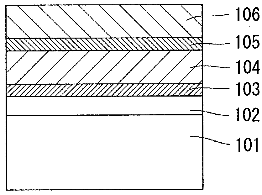
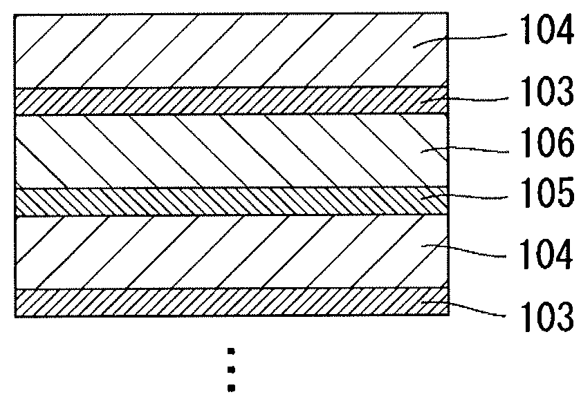
[0027]As shown in FIG. 1, a nitride semiconductor multilayer film reflector is fabricated. In the reflector, a second composition-graded AlGaN layer (a second composition-graded layer) 103 / an Al0.5Ga0.5N layer (a first semiconductor layer) 104 and a first composition-graded AlGaN layer (a first composition-graded layer) 105 / a GaN layer (a second semiconductor layer) 106 are paired and are stacked sequentially in this order into a layered structure. The Al0.5Ga0.5N is selected as the first semiconductor layer 104. The GaN is selected as the second semiconductor layer 106. When the first semiconductor layer 104 has an excessively high Al composition value, a lattice mismatch with the GaN as the second semiconductor layer 106 becomes excessively large, so that the crystallinity deteriorates and a reflectance is reduced with this. Contrarily, when the first semiconductor layer 104 has an excessively low Al composition value, a refractive index difference between the first and second sem...

embodiment 2

[0052]The nitride semiconductor multilayer film reflector is fabricated which includes pairs of stacked structures each one of which pairs includes a second composition-graded AlInN layer (the second composition-graded layer) 501 / an Al0.85In0.15N layer (the first semiconductor layer) 502 and an first composition-graded AlInN layer (the first composition-graded layer) 503 and the GaN layer (the second semiconductor layer) 106, as shown in FIG. 7. Embodiment 2 differs from embodiment 1 in the use of AlInN, instead of AlGaN, in the first semiconductor layer 502, the first composition-graded layer 503 and the second composition-graded layer 501. Al0.85In0.15N is selected as the first semiconductor layer 502. GaN is also selected as the second semiconductor layer 106 in the same manner as in embodiment 1. The Al composition value of the first semiconductor layer 502 may be 0.83 in order that the first semiconductor layer 502 may be lattice-matched with the GaN. However, compressive strai...

embodiment 3

[0063]The nitride semiconductor multilayer film reflector is fabricated which includes 49.5 pairs of stacked structures each one of which pairs includes a second composition-graded AlGaN layer (the second composition-graded layer) 601 / an Al0.82In0.18N layer (the first semiconductor layer) 602 and a first composition-graded AlGaN layer (the first composition-graded layer) 603 / the GaN layer (the second semiconductor layer) 106, as shown in FIG. 9. Embodiment 3 differs from embodiment 2 in the use of AlGaN, instead of AlInN, in the first composition-graded layer 603 and the second composition-graded layer 601. Al0.02In0.18N is selected as the first semiconductor layer 602. GaN is also selected as the second semiconductor layer 106 in the same manner as in embodiments 1 and 2. The Al composition value of the first semiconductor layer 602 may be set to 0.83 in order to be lattice-matched with the GaN. However, tensile strain is inherent in the first composition-graded AlGaN layer 603 and...


PUM


Abstract

Achieving resistance reduction of a nitride semiconductor multilayer film reflector. In the nitride semiconductor multilayer film reflector, a first semiconductor layer (104) has a higher Al composition than a second semiconductor layer (106). A first composition-graded layer (105) is interposed between the first and second semiconductor layers (104, 106) so as to be located at a group III element face side of the first semiconductor layer (104), the first composition-graded layer (105) being adjusted so that its Al composition becomes lower as coming close to the second semiconductor layer (106). A second composition-graded layer (103) is interposed between the first and second semiconductor layers (104, 106) so as to be located at a nitride face side of the first semiconductor layer (104). The second composition-graded layer (103) is adjusted so that its Al composition becomes lower as coming close to the second semiconductor layer (106). Energy levels of electrons at bottoms of conduction bands of the first and second semiconductor layers (104, 106) and the first and second composition-graded layers (105, 103) are continuous without band offset. The first composition-graded layer (105) has an n-type impurity concentration of not less than 5×1019 cm−3.

Description

TECHNICAL FIELD[0001]The present invention relates to a nitride semiconductor multilayer film reflector and a light-emitting device using the same.BACKGROUND ART[0002]An AlGaAs surface-emitting semiconductor laser device extracting laser light from a direction perpendicular to a substrate surface has semiconductor multilayer film reflectors in a vertical direction of an active layer, in order to make up an optical resonator. The semiconductor multilayer film reflector is configured of first and second semiconductor layers which are stacked alternately and have respective bandgap energies larger than energy corresponding to an oscillation wavelength of laser light.[0003]In the semiconductor multilayer film reflector, the first and second semiconductor layers having a large refractive index difference, namely, a large bandgap energy difference therebetween are selected in order to realize a high reflectance. This results in a higher heterojunction barrier produced on a junction of the...

Claims


Application Information

Patent Timeline
Patent Type & Authority Applications(United States)
IPC IPC(8): H01L33/10H01L33/32
CPCH01L33/32H01L33/10H01S5/18361H01S5/34333H01L33/06H01L33/14H01L33/0075
Inventor TAKEUCHI, TETSUYAIWAYA, MOTOAKIAKASAKI, ISAMU
Owner MEIJO UNIVERSITY
Why Eureka
Try Eureka