

Method of making photovoltaic devices with reduced conduction band offset between pnictide absorber films and emitter films
a technology of pnictide absorber and emitter film, which is applied in the manufacture of semiconductor/solid-state devices, semiconductor devices, electrical devices, etc., can solve the problems of increasing the degree of lattice mismatch between the absorber and the emitter film, and achieve the effect of reducing the conduction band offs
- Summary
- Abstract
- Description
- Claims
- Application Information
AI Technical Summary
Benefits of technology
Problems solved by technology
Method used
Image

Examples
example 1
Substrate Preparation
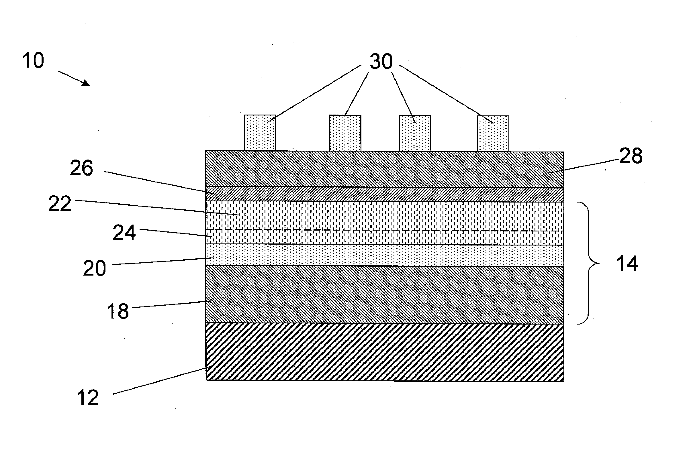
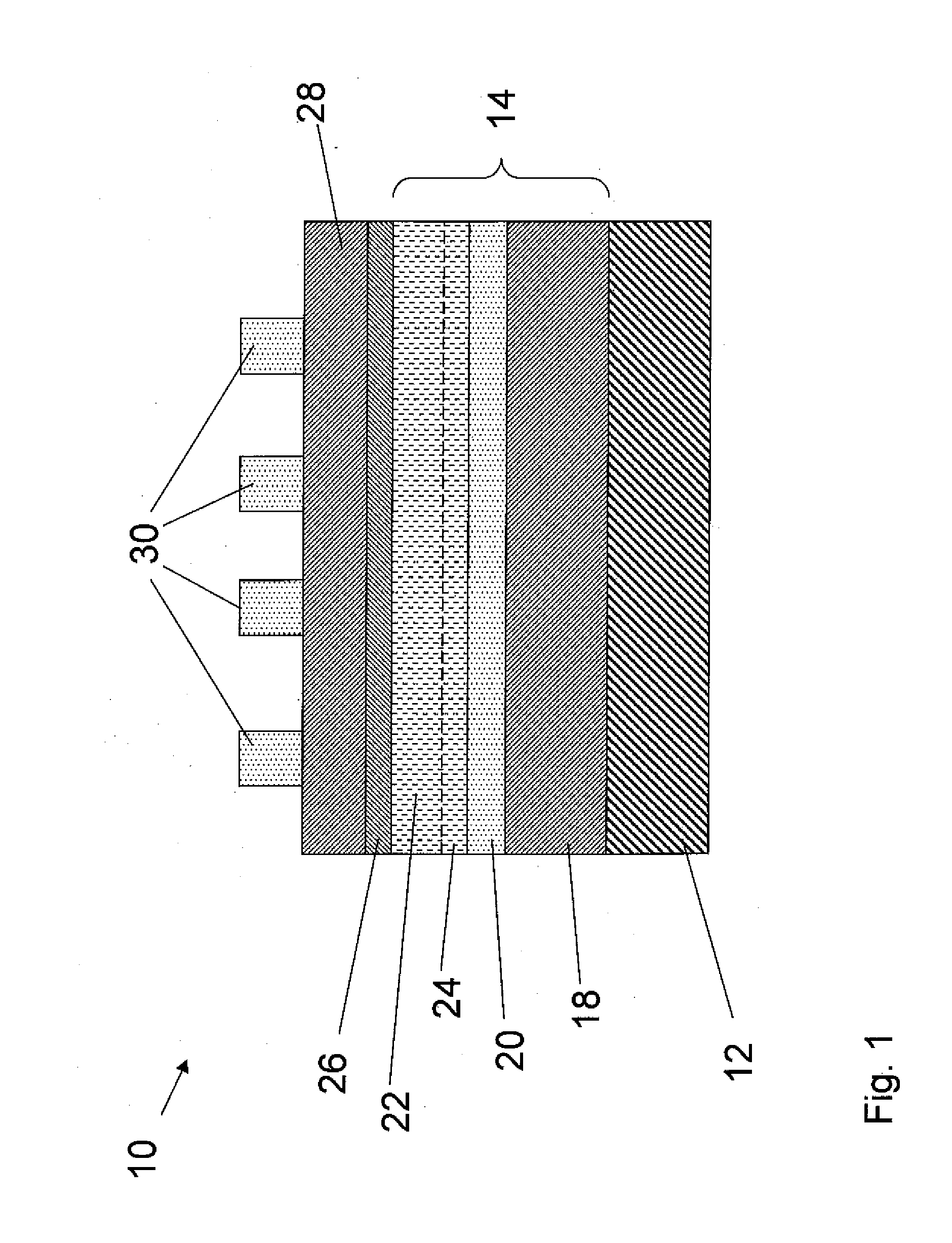
[0072]A solid state ZnS / Zn3P2 heterjunction solar cell is fabricated on a degeneratively doped, p-type, GaAs (001) single crystal substrate using compound source, molecular beam epitaxy (MBE) techniques according to techniques and a corresponding apparatus that practices these techniques are described in more detail in co-pending U.S. Provisional Patent Application titled METHODOLOGY FOR FORMING PNICTIDE COMPOSITIONS SUITABLE FOR USE IN MICROELECTRONIC DEVICES, Ser. No. 61 / 441,997, filed Feb. 11, 2011, in the names of Kimball et al., and having Attorney Docket No 70360 (DOW0039P1). The growth is performed in ultra high vacuum (UHV) molecular beam epitaxy chamber with a base pressure of 10−10 torr. The chamber is equipped with compound sources of Zn3P2 and ZnS, as well as elemental sources of Al, Ag, Zn, and Mg.
[0073]The backside of the GaAs substrate is coated with a Pt—Ti—Pt low resistivity back contact prior to cell fabrication. The substrate is mounted to a m...
example 2
[0075]Zinc phosphide film growth is performed by subliming 99.9999% Zn3P2 from a Knudsen effusion cell. The effusion cell is heated to above 350° C., providing a beam pressure between 5×10⁻⁷ and 2×10⁻⁶ Torr as determined by a translatable nude ionization gauge. The growth is performed at a substrate temperature of 200° C. The film deposition rate is about 0.3 to 1.0 angstroms / s. A typical film thickness is 400 to 500 nm. Thicker films are possible but require longer growth rates or higher beam pressures. Elemental Ag is incorporated as a dopant during the growth process by co sublimation from an additional Ag source. The Ag source is operated between 700° C. and 900° C. Immediately after Zn3P2 growth, the substrate temperature is decreased to the ZnS deposition temperature.
example 3
Tuned ZnS Growth
[0076]ZnS growth is performed using a Knudsen effusion cell containing 99.9999% ZnS. The effusion cell is heated to 850° C. for deposition. This creates a beam pressure of about 1.5×10⁻⁶ Torr. During ZnS growth, the substrate is held at 100° C. Under this beam pressure and substrate temperature, ZnS growth rate is about 1 angstrom / s. A film having a thickness of 100 nm is grown. During growth, Al and Mg are co-introduced with the ZnS. Al is provided using an electron beam evaporator filled with 99.9999% Al metal. The extent of Al incorporation and therefore dopant density is controlled by the power supplied to the evaporator. The Al density in the grown film is typically between 1×10¹⁸ and 1×1019 cm−3. Mg is provided using an effusion cell filled with 99.9999% Mg with operating temperature between 300° C. and 600° C. Mg is co-introduced only during the first 10 to 100 nm of film growth. In alternative embodiments, Mg could be included throughout the ZnS film.
PUM
 Abstract
Description
Claims
Application Information