Spectrally and Temporally Engineered Processing using Photoelectrochemistry

a technology of photoelectrochemistry and spectrally and temporally engineered processing, which is applied in the direction of microstructured devices, semiconductor/solid-state device testing/measurement, instruments, etc., can solve the problems of difficult to achieve three-dimensional structures with multiple heights using conventional photolithography and etching, static gray-scale masks, and high cost, so as to reduce the resistance of an ohmic contact

Active Publication Date: 2016-04-28
THE BOARD OF TRUSTEES OF THE UNIV OF ILLINOIS
View PDF5 Cites 7 Cited by
  • Summary
  • Abstract
  • Description
  • Claims
  • Application Information

AI Technical Summary

Benefits of technology

[0056]creating an adiabatic taper between an active section and a passive section by displaying a gradient pattern of light intensity to slowly vary the etch height; and

Problems solved by technology

Three-dimensional structures with multiple heights are difficult to achieve using conventional photolithography and etching.
These masks, however, have a limited number of gray levels, are very expensive since the cost scales with the number of levels, and may require several iterative purchases while a given process is perfected.
More importantly, gray-scale masks are static and thus cannot easily be modified if the design dimensions or device layout is changed.
Serial laser writing, however, requires precise scanning equipment and software control, and the throughput is relatively low.
Although surface topography can be transferred to a semiconductor or other substrate with an etch of appropriate selectivity, it is difficult to transfer the topography of free standing structures with this method or to use the method to perform other types of semiconductor processing, e.g. doping or metallization.

Method used


Image

  • Spectrally and Temporally Engineered Processing using Photoelectrochemistry
  • Spectrally and Temporally Engineered Processing using Photoelectrochemistry
  • Spectrally and Temporally Engineered Processing using Photoelectrochemistry

Examples


example i

Unprocessed Wafer

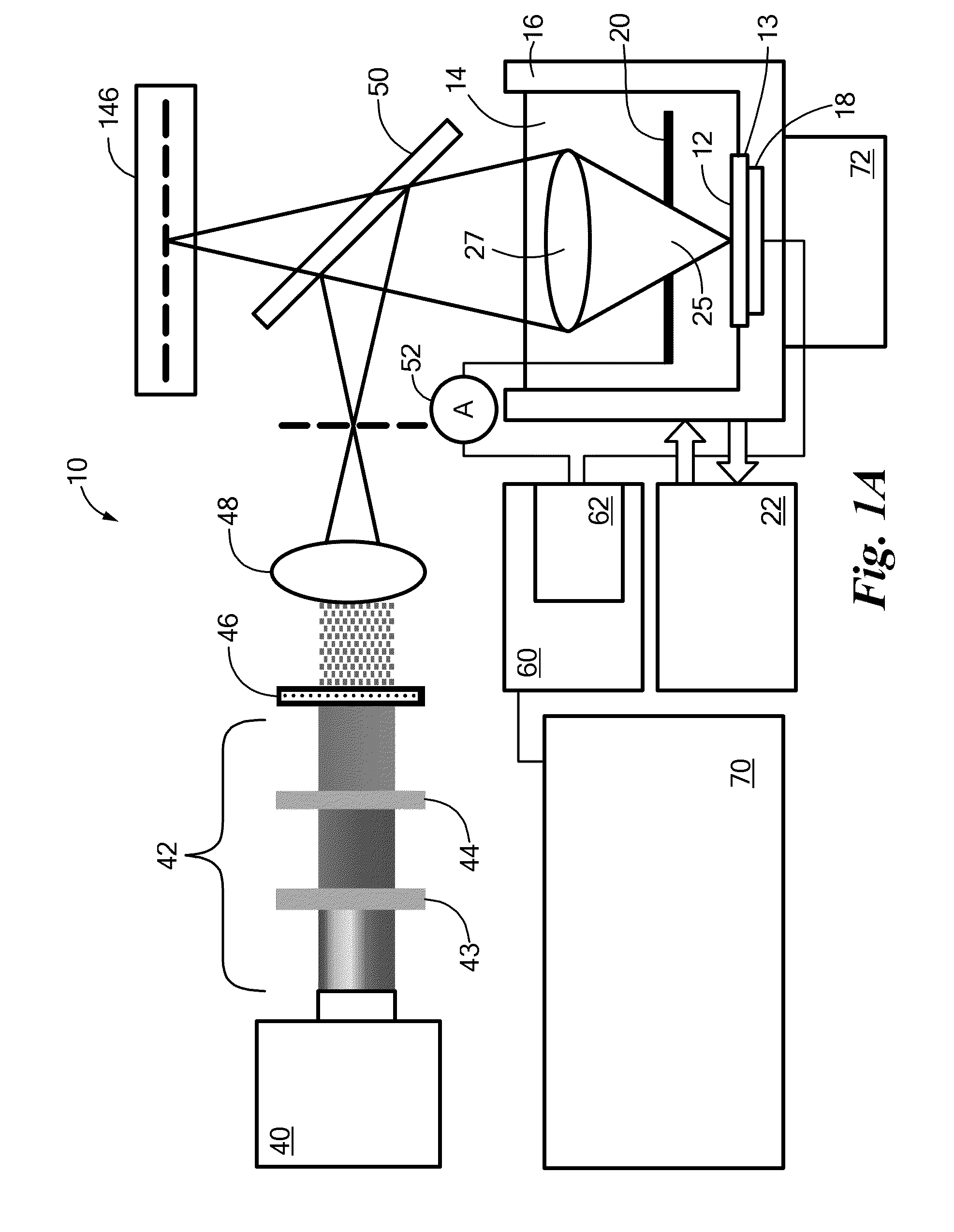
[0128]In accordance with embodiments of the present invention, epi-DPM may provide accurate topographic height maps relative to other points in the image and therefore may be advantageously made insensitive to any common mode motion of the sample. To characterize the spatial and temporal path length noise of the epi-DPM method described herein, a plain, unprocessed n+ GaAs wafer (heavily n-doped) was imaged repeatedly in succession. The successive imaging yielded a time-lapse series of images containing 256 frames at 8.93 frames / s. A 10× objective (NA=0.25) provided a lateral resolution of 1 μm, with a field of view of approximately 160 μm×120 μm. After recovering the height images, a quadratic fit of each individual image was subtracted off. The linear portion of the fit corrects for the tilt of the sample and the angle of interference in camera plane 148 while the quadratic portion corrects for the quadratic phase front of the beam across the field of view. After ...

example ii

Photochemical Etching of Arrays of Microlenses

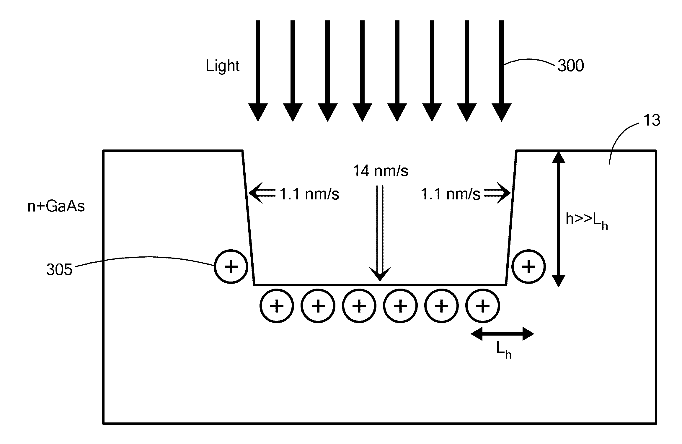
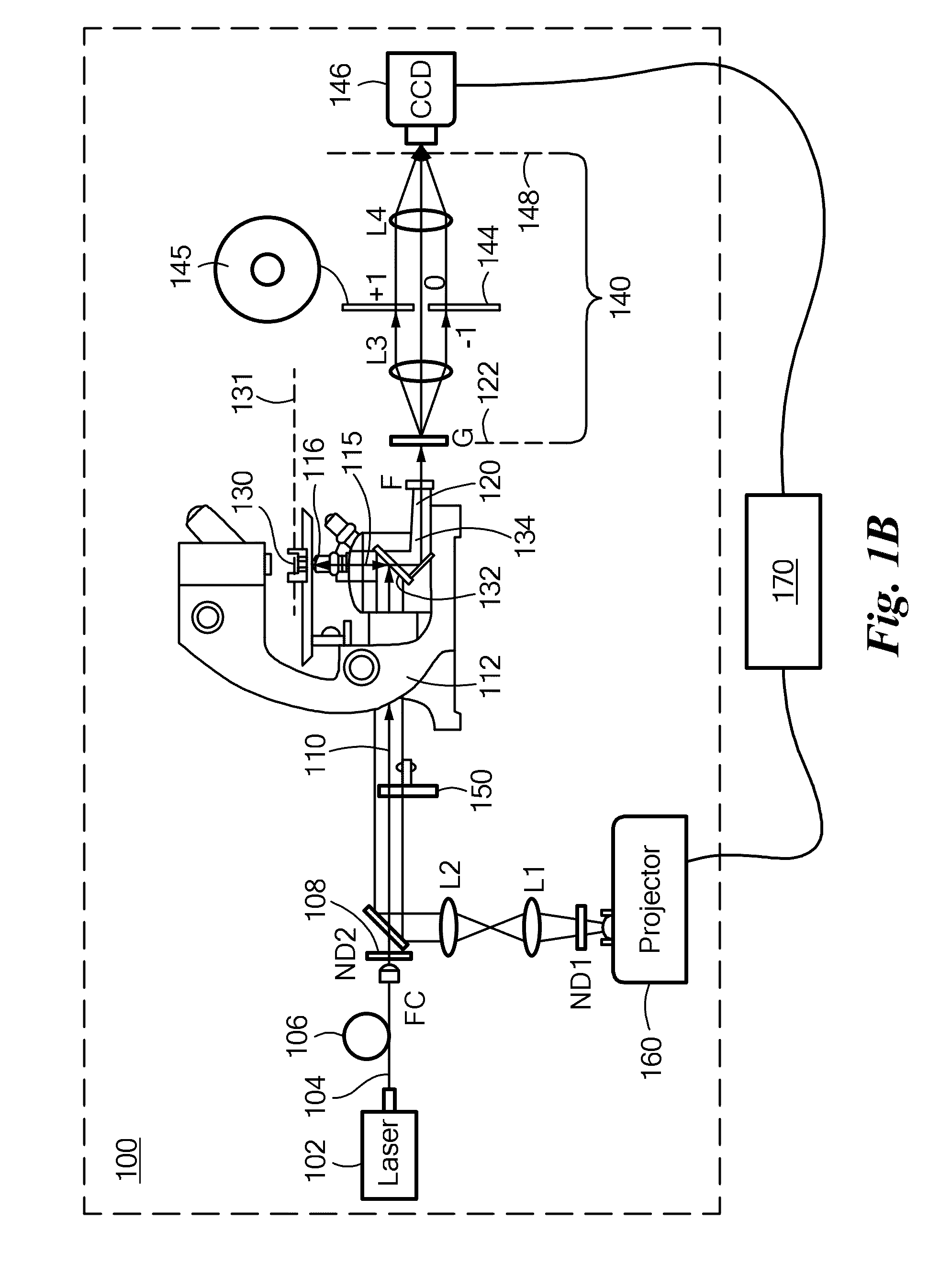
[0129]As an example of photochemical etching capabilities, epi-DPM was used to image microlens structures fabricated by photochemical etching. Light produced by light projector 160 (EPSON Powerlite S5 EMP-S5, for example) in the illumination path, such that gray-scale or color images delivered by a computer can be mapped onto the sample, as shown in FIG. 1B. Individual microlenses were fabricated using a digital image as an optical mask, which may be implemented by a spatial light modulator (SLM), for example, in order for the mask to be programmable and amenable to modification in real time. FIG. 5A shows a pattern of specified intensity distribution (otherwise referred to as mask 500) delivered by projector 160 to sample plane 131 (shown in FIG. 1B), while FIG. 5B is the corresponding epi-DPM image of the resulting fabricated microlens. Projector 160 may also deliver a pattern of both specified intensity distribution and specified colo...


PUM

PropertyMeasurementUnit
depthaaaaaaaaaa
depthaaaaaaaaaa
dark etch rateaaaaaaaaaa

Abstract

Methods and apparatus for subtractively fabricating three-dimensional structures relative to a surface of a substrate and for additively depositing metal and dopant atoms onto the surface and for diffusing them into the bulk. A chemical solution is applied to the surface of the semiconductor substrate, and a spatial pattern of electron-hole pairs is generated by projecting a spatial pattern of illumination characterized by a specified intensity, wavelength and duration at each pixel of a plurality of pixels on the surface. An electrical potential is applied across the interface of the semiconductor and the solution with a specified temporal profile relative to the temporal profile of the spatial pattern of illumination. Such methods are applied to the fabrication of a photodetector integral with a parabolic reflector, cell size sorting chips, a three-dimensional photonic bandgap chip, a photonic integrated circuit, and an integrated photonic microfluidic circuit.

Description

[0001]The present application is a continuation-in-part of U.S. Ser. No. 13 / 630,286, incorporated herein by reference, and now issued as U.S. Pat. No. ______.[0002]This invention was made with government support under Grants CBET 1040462, ECCS 1509609, and EEC 1407194 awarded by the National Science Foundation. The Government has certain rights in the invention.TECHNICAL FIELD[0003]The present invention relates to methods and apparatus for maskless photochemical etching of materials, and, more particularly, to photochemical etching of three-dimensional structures in semiconductors.BACKGROUND ARTDefinitions[0004]“Grayscale topography,” in the context of semiconductor device fabrication, is a defined term referring to the field of variable height three-dimensional nanostructures patterned into a substantially planar surface. The term “variable height” is defined to mean that the depth of features relative to a fiducial plane is a function of displacement within the plane. Thus, height...

Claims


Application Information

Patent Timeline
Patent Type & Authority Applications(United States)
IPC IPC(8): H01L21/306H01L31/0236H01L21/768H01L31/0232
CPCH01L21/30604H01L21/76886H01L31/02363H01L31/02327G01B11/2441H01L22/12C25F3/14C25F3/12H01L21/30617B81C1/00103H01L21/3063B81C1/00111B81C1/00214B81C1/00484B81C1/00119B81C1/00539B81C2201/0139B81C1/00595B81C2201/0157B81C2201/0114
Inventor GODDARD, LYNFORDWANG, KAIYUANEDWARDS, CHRISEDWARDS, LONNAYU, XINLIU, GANG LOGANWASHINGTON, SAMUELSRIVASTAVA, SHAILENDRAKOKER, TERRYLEE, JULIANNECARLSON, CATHERINE BRITT
Owner THE BOARD OF TRUSTEES OF THE UNIV OF ILLINOIS
Why Eureka
Try Eureka