Design Support System, Design Support Method and Design Support Program

a design support and design technology, applied in the field of systems and methods to support the design of electrical equipment, can solve the problems of compromising the accuracy of calculation, requiring considerable calculation time, and requiring simulation of the whole pcb plane, so as to reduce the electromagnetic radiation from the pcb, reduce the calculation time, and reduce the effect of electromagnetic radiation from the edges

Inactive Publication Date: 2016-06-02
HITACHI LTD
View PDF0 Cites 7 Cited by
  • Summary
  • Abstract
  • Description
  • Claims
  • Application Information

AI Technical Summary

Benefits of technology

[0022]Another aspect is that the effect of current bypass devices on the radiation is approximately estimated based on the ratio of the power of the radiation effective wave injected into infinite planes without and with the current bypass devices.
[0023]Another aspect is that the selection of the position and values of current bypass devices can be automatized. When it is made by the user it is facilitated by plots of the horizontal distribution of the voltage between the bottom and top planes. Given the PCB layout close to a noise source device (LSI), the present invention helps the user to select a suitable configuration of current bypass devices for reducing the electromagnetic radiation from the PCB edges.
[0024]The most advantageous effect of the present invention is that the design of electrical equipment, such as PCBs, with lower electromagnetic radiat

Problems solved by technology

One problem of this method is that simulations of the whole PCB planes are required, including all the components connected to the planes.
Although very important progresses have been made recently in PCB simulation techniques, this still req

Method used


Image

  • Design Support System, Design Support Method and Design Support Program
  • Design Support System, Design Support Method and Design Support Program
  • Design Support System, Design Support Method and Design Support Program

Examples


embodiment 1

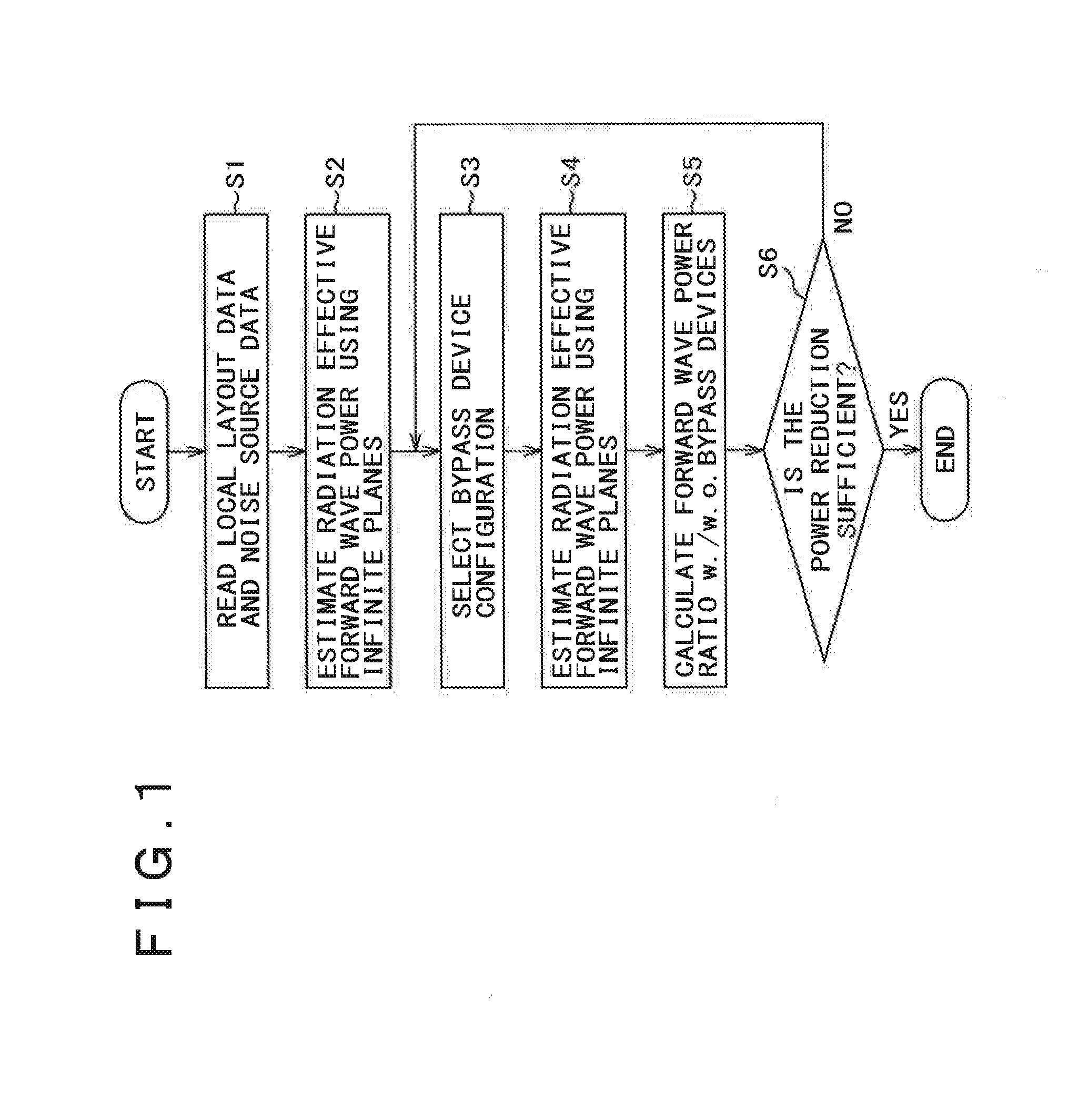
[0088]The main embodiment is described in FIG. 1, whereas the selection of the position of the current bypass devices and the decision whether the power reduction is sufficient or not, are made by the user.

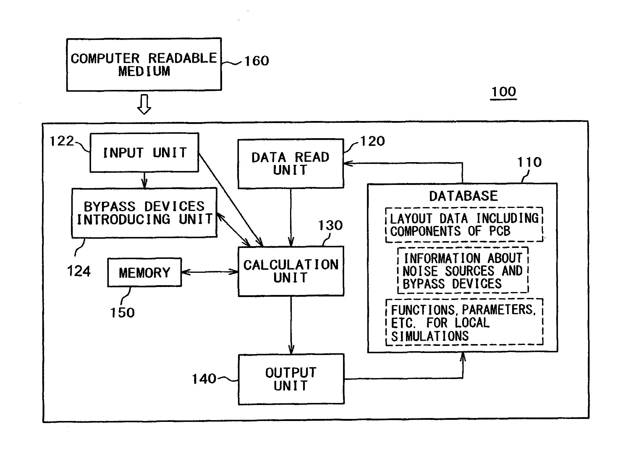
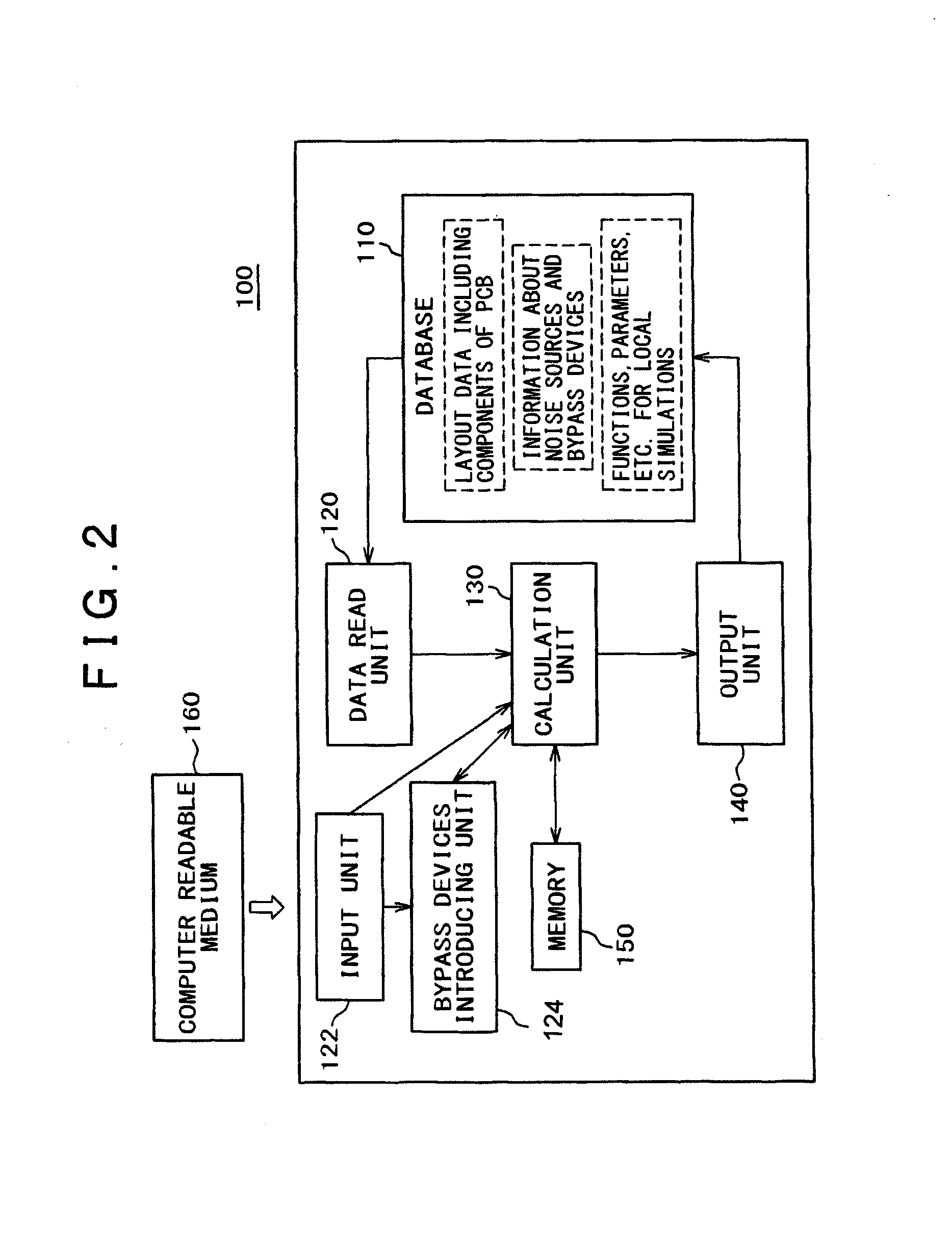
[0089]FIG. 2 is a diagram for showing an embodiment of a design support system 100 to support design of electrical equipment, according to the present invention. For the system 100, a computer may be used to implement the method described in FIG. 1.

[0090]The system 100 comprises;

[0091]a database 110 for storing layout data, noise source (a noise source device and noise source elements) data of the simulation model of a printed circuit board having assumed infinite power supply planes, and calculation results;

[0092]an input unit 120 for imputing data to the database 110, for example, layout data including components of the PCB model, information about noise sources, bypass devices, and necessary data for local simulations, such as functions, parameters, etc.;

[0093]a calculation uni...

second embodiment

[0119]According to a second embodiment, in the second and fourth steps (S2 and S4) in FIG. 1, the radiation effective forward wave voltage in the observation location is calculated with methods different from that described in the Non Patent Document 3. Alternative techniques can use for example a different via model, or a different algorithm for connecting in cascade the single plane pairs, such as ABCD-matrices or transmission (T-) matrices instead of the Y-matrix. Completely different numerical techniques can be also used, for example the method of moments (MoM), or even the finite element method (FEM), the finite difference method (FDM) in time or frequency domain, the finite integration method (FIM), as long as absorbing boundary conditions are used for the external boundaries, simulating in this way the conditions of infinite planes.

third embodiment

[0120]According to a third embodiment, in the sixth step (S6) in FIG. 1, the decision whether the reduction is sufficient or not, and the selection of the new configuration of current bypass devices in the third step (S3) are made automatically with an optimization procedure. For example genetic algorithms can be used for selecting the new configuration. The decision can be made based on a target reduction that the user can select before starting the optimization. Alternatively, the optimization can aim to reach the minimum radiation effective forward wave power within a constrained space selected by the user before starting the optimization. The radiation effective forward wave power can be estimated with the methods described in the first and second embodiments.


PUM


Abstract

A design support system for designing a printed circuit board, comprising: a database for storing layout data, noise source data of the printed circuit board, and calculation results; a data reading unit for reading noise source data and local layout data of a local area around the noise source from the database; a bypass devices introducing unit for introducing current bypass devices to the local area, and a calculation unit for estimating the radiation effective forward wave power injected into assumed infinite power supply planes of the printed circuit board from the noise source without and with current bypass devices, and for calculating their ratio.

Description

FIELD OF THE INVENTION[0001]This invention relates to systems and methods to support design of electrical equipment, in particular to support the design of printed circuit boards with low electromagnetic emissions.BACKGROUND OF THE INVENTION[0002]Power supply noise of printed circuit boards (PCBs) is a source of high frequency electromagnetic interferences (EMI), and it is mainly generated by simultaneous switching of large scale of integration (LSI) integrated circuits (ICs) (LSI-ICs in short LSIs). FIG. 3 is a longitudinal section view of an example of a PCB 20 with two planes (a power plane 23 and a ground plane 24 in dielectric 22), LSI 21, via 25, and bypass capacitors 26. The simultaneous switching noise (SSN) propagates as an electromagnetic (EM) noise wave 27 between the power supply planes (23, 24) and most of it is reflected back as reflected wave 29 by the board edges (28), creating resonances that are dependent on the board layout as shown in FIG. 3.[0003]In order to red...

Claims


Application Information

Patent Timeline
IPC IPC(8): H05K3/00G06F17/50
CPCG06F17/5072H05K3/0005G06F2119/10G06F30/367G06F30/392
Inventor PAOLETTI, UMBERTOKOMIYA, YASUMARO
Owner HITACHI LTD
Why Eureka
Try Eureka