Semiconductor integrated circuit device and wearable device

a technology of integrated circuit and semiconductor, which is applied in the field of semiconductor integrated circuit devices and wearable devices, can solve the problems of increased cost of portable terminal devices, high effect not expected with respect to low power consumption etc., and achieves increased cost of portable terminal devices, high effect, and increased number of mounted semiconductor devices

Active Publication Date: 2016-06-23
RENESAS ELECTRONICS CORP
View PDF4 Cites 13 Cited by
  • Summary
  • Abstract
  • Description
  • Claims
  • Application Information

AI Technical Summary

Benefits of technology

[0008]In the configuration in which two semiconductor devices (that is, the semiconductor device having the main CPU built-in and the semiconductor device having the sub CPU built-in) are used, there is a concern about that the number of the mounted semiconductor devices is increased and the cost of the portable terminal device is increased. In addition, in the configuration in which the DVFS technique is used, even when the frequency is lowered to perform the operation at a low speed, a standby current caused by a leakage current is not reduced, so that a high effect is not expected with respect to the low power consumption. Furthermore, a changeable frequency range is about 50% depending on the DVFS technique, and the frequency cannot be changed in a unit of digit. As a result, a high effect is not expected with respect to the low power consumption.

Problems solved by technology

In the configuration in which two semiconductor devices (that is, the semiconductor device having the main CPU built-in and the semiconductor device having the sub CPU built-in) are used, there is a concern about that the number of the mounted semiconductor devices is increased and the cost of the portable terminal device is increased.
In addition, in the configuration in which the DVFS technique is used, even when the frequency is lowered to perform the operation at a low speed, a standby current caused by a leakage current is not reduced, so that a high effect is not expected with respect to the low power consumption.
As a result, a high effect is not expected with respect to the low power consumption.
In the configuration in which a substrate bias voltage supplied to the substrate of the semiconductor device is changed, it is difficult to stably operate the semiconductor device.

Method used


Image

  • Semiconductor integrated circuit device and wearable device
  • Semiconductor integrated circuit device and wearable device
  • Semiconductor integrated circuit device and wearable device

Examples


first embodiment

Overall Configuration of Semiconductor Device

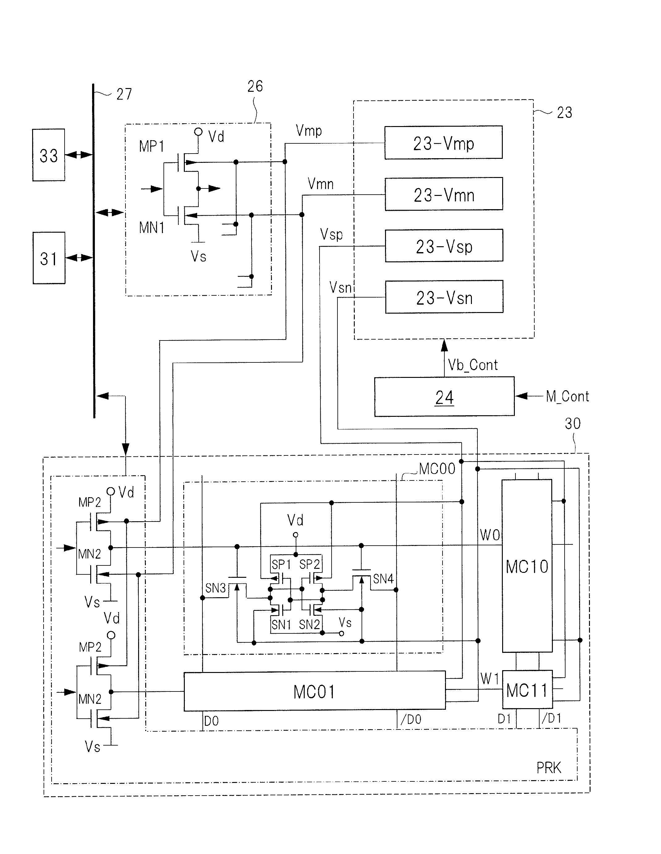
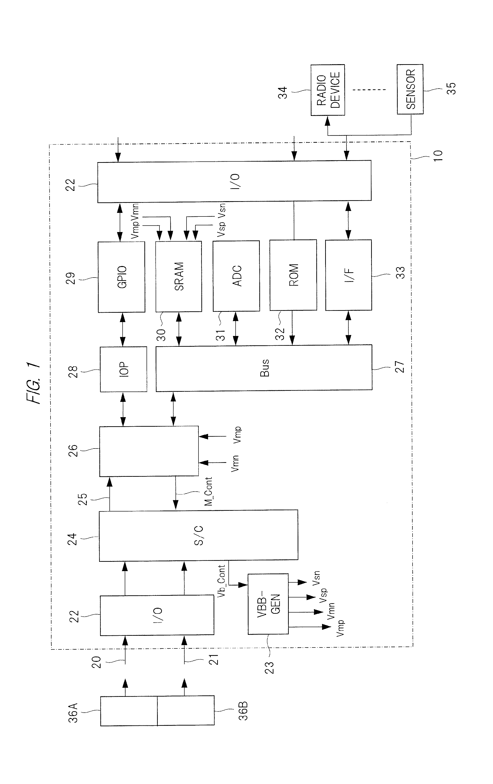
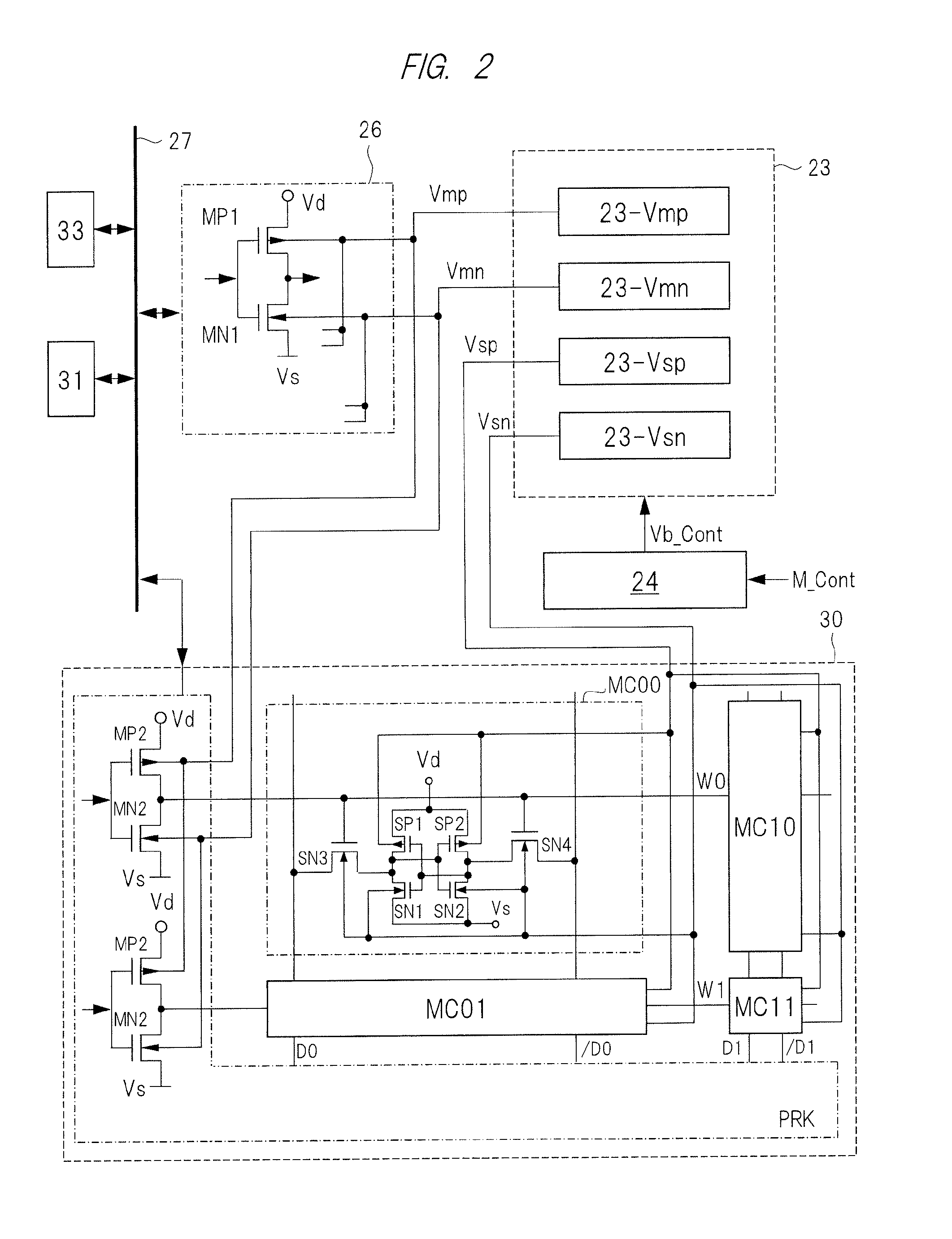
[0033]FIG. 1 is a block diagram illustrating a configuration of a semiconductor device 10 according to a first embodiment. In this drawing, the block surrounded by a dashed line indicates a circuit formed by one semiconductor chip and a bus. The semiconductor device 10 includes a central processing unit (CPU) 26, a GPIO 29, an SRAM 30, an ADC 31, a read only memory (ROM) 32, an I / F 33, an S / C 24, an I / O 22, an IOP 28, and a VBB-GEN 23. Here, the I / O 22 indicates an input / output circuit, and includes a circuit for converting a voltage level of a signal between the outside and the inside of the semiconductor device 10, a circuit for buffering the signal and the like, which are not particularly limited.

[0034]In FIG. 1, the GPIO 29 is a general purpose input / output circuit, and the microprocessor (CPU) 26 accesses the GPIO 29 through the control circuit IOP 28. The GPIO 29 transmits and receives information with respect to the outside of the ...

second embodiment

[0127]The semiconductor device according to a second embodiment is different from the first embodiment in that the voltage value of the substrate bias voltage generated by the substrate bias generation circuit 23 is changed. The configuration of the semiconductor device is the same as that of the first embodiment except that the number of substrate bias generation circuits is changed. The operation of the substrate bias circuit 23 is the same as that of the first embodiment, and the description thereof will not be repeated.

[0128]FIG. 9 is a characteristic diagram illustrating the characteristics of the P-type SOTB transistor and the N-type SOTB transistor according to the second embodiment. Similarly to FIG. 5, FIG. 9 illustrates a characteristic of the changes of the threshold voltages of the P-type SOTB transistors SP1 and SP2 and the N-type SOTB transistors SN1 to SN4 when the substrate bias voltages Vsp and Vsn are changed.

[0129]In this drawing, the broken line indicates a chang...


PUM


Abstract

To provide a semiconductor device which can be stably operated while achieving a reduction of the power consumption.
A semiconductor device includes a CPU, a system controller which designates an operation speed of the CPU, P-type SOTB transistors, and N-type SOTB transistors. The semiconductor device is provided with an SRAM which is connected to the CPU, and a substrate bias circuit which is connected to the system controller and is capable of supplying substrate bias voltages to the P-type SOTB transistors and the N-type SOTB transistors. Here, when the system controller designates a low speed mode to operate the CPU at a low speed, the substrate bias circuit supplies the substrate bias voltages to the P-type SOTB transistors and the N-type SOTB transistors.

Description

CROSS-REFERENCE TO RELATED APPLICATION[0001]The present application claims priority from Japanese Patent Application No. 2014-255557 filed on Dec. 17, 2014, the content of which is hereby incorporated by reference into this application.TECHNICAL FIELD OF THE INVENTION[0002]The present invention relates to a semiconductor integrated circuit device and a wearable device, and particularly to a semiconductor integrated circuit device which is suitable to reduce power consumption.BACKGROUND OF THE INVENTION[0003]As a wearable device, there is a portable terminal device which is mounted on a wrist such as a smart watch. Such a portable terminal device is driven by power supplied from a battery, and is required to work for a long time. In order to achieve a function of the terminal and a function of the wrist watch, the portable terminal device is mounted with a semiconductor integrated circuit device (hereinafter, simply referred to as a semiconductor device) in which a microprocessor (he...

Claims


Application Information

Patent Timeline
Patent Type & Authority Applications(United States)
IPC IPC(8): G11C11/417
CPCG11C11/417H01L27/1207G11C5/146H01L27/1203G11C11/41G11C11/413G11C5/148H10B10/12H10B10/18G04G21/025H01L27/092H04B1/385
Inventor KAMOHARA, SHIROYAMAGATA, YASUSHIHASEGAWA, TAKUMISUGII, NOBUYUKI
Owner RENESAS ELECTRONICS CORP
Why Eureka
Try Eureka