
Unknown

a technology of capacitors and dielectric structures, applied in the field of capacitors, can solve the problems of increasing the bending of the disk, the bending of the semiconductor disk, and the increase of the cost per device approximately linearly to the increasing chip surface, so as to reduce reduce the effect of bending or preventing the propagation of defects

Active Publication Date: 2016-06-30
FRIEDRICH ALEXANDER UNIV ERLANGEN NURNBERG +1
View PDF7 Cites 10 Cited by
  • Summary
  • Abstract
  • Description
  • Claims
  • Application Information

AI Technical Summary

Benefits of technology

The invention presents a method for producing a capacitor with a high integration density and a high capacitance without compromising the processability of the semiconductor substrate. This is achieved by generating dielectric layers with opposite material tences that reduce or prevent bending of the substrate during production. A dielectric layer can be formed in a trench of the substrate using a two-step process to prevent defects and improve reliability. Furthermore, the invention allows high thicknesses of the dielectric structure and a high number of degrees of freedom in material selection and dielectric layer order. The produced capacitor can be used in power modules or coupling capacitors with high integration and high functionality.

Problems solved by technology

As it is common in semiconductor technology, the costs per device increase approximately linearly to the increasing chip surface.
When producing such MIS capacitors, this results in a strong bending of the semiconductor disk resulting from the mechanical tensions (mechanical stress) in the layers and the underlying substrate.
With increasing surface enlargement, bending of the disk increases so much that further processing (in particular after removing the layers from the rear of the semiconductor disk) is no longer possible due to the mechanical bending.
Thus, bending of the semiconductor disk to that extent represents a barrier for introducing monolithically integrated capacitors and RC elements with high integration density for operating voltages of 600 Volt and more.
However, only very thin dielectrics (up to 30 nm) and trenches having diameters in the sub-micrometer range are used there, since a dielectric strength of approximately 10 Volts may not be exceeded.
In such thin dielectrics, bending of the semiconductor disk only occurs to a very limited extent.
The dielectric strength of the dielectrics in such layers is, however, limited to below 30 Volt.
So far, monolithically integrated capacitors having operating voltages in the range of 200 Volt and more are not available.
However, the used layer stacks are not sufficient for applications with operating voltages of up to 600 Volt.
Previous findings, however, show that already with a small surface enlargement, devices having such a layer stack can no longer be produced.
Even production on a planar surface does not seem to be possible since the high mechanical tensions of the layers have the effect that the same chip off from the surface or cracks are formed that propagate into the substrate.
Further, the low obtainable capacitance also opposes the production of devices on a planar surface or as trench capacitor with a small surface enlargement.
So far, there has been no success in producing monolithically integrated capacitors with an effective layer thickness dCET allowing a surface enlargement V according to the formula
However, since the surface enlargement decreases with the square of the distance of the centers of the holes, this method is disadvantageous when a capacitance per chip area that is as high as possible is to be realized.
In particular, for realizing monolithically integrated RC elements, this method has the disadvantage that due to the structuring and the dielectric on the bottom of the device, heat dissipation from the volume of the semiconductor disk is significantly reduced.
This allows the production of devices having a respectively high dielectric strength, but is disadvantageous for cost-effective realization.
However, due to the very low leakage currents of monolithically integrated capacitors, a deviation of the parallel resistors by a factor of more than 2 is to be expected.
Here, however, the additional layer, on the one hand, increases the production process effort and, on the other hand, claims additional volume in the hole structures, whereby the obtainable surface enlargement is reduced or cannot be fully utilized.
For this reason, this layer cannot contribute to preventing wafer bending during the whole process.

Method used


Image

  • Unknown
  • Unknown
  • Unknown

Examples


Embodiment Construction

[0045]Before embodiments of the present invention will be discussed in detail based on the drawing, it should be noted that identical, functionally identical or equivalent elements, objects and / or structures in the different figures are provided with the same reference numbers, so that the description of these elements illustrated in different embodiments can be interchanged or can be applied to one another.

[0046]In the following, reference is made to intrinsic and thermal material tensions Δ. Thermal material tensions Δ are explained such that based on positive coefficients of thermal expansion α materials shrink with respect to an adjacent layer and / or a (semiconductor) substrate during cooling. It is obvious that heating can result in an expansion. Further, the following statements can also be understood such that materials perform a negligible deformation during heating or cooling, i.e., the coefficient of expansion is approximately zero. Alternatively, the coefficient of therma...


PUM


Abstract

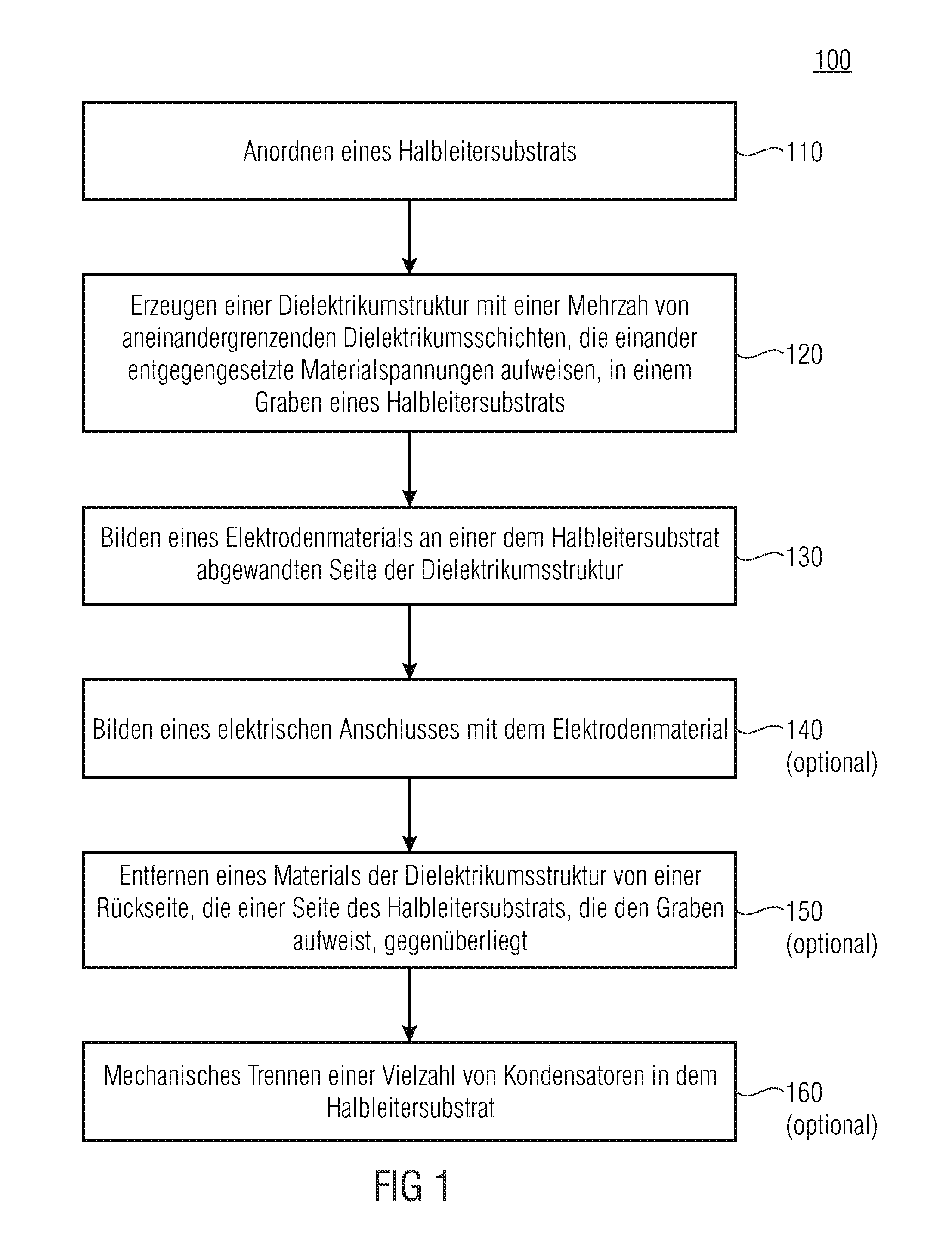
In a method for producing a capacitor, a dielectric structure is generated in a trench of a semiconductor substrate. The dielectric structure includes a plurality of adjacent dielectric layers having opposing material tensions.

Description

CROSS-REFERENCE TO RELATED APPLICATIONS[0001]This application claims priority from German Patent Application No. 10 2014 223 904.4, which was filed on Nov. 24, 2014, and is incorporated herein in its entirety by reference.BACKGROUND OF THE INVENTION[0002]The present invention relates to a capacitor with a semiconductor substrate and to a method for producing the same. Further, the present invention relates to stress compensation in monolithic trench capacitors for power electronic applications for increasing the integration density.[0003]Monolithic integrated capacitors and RC elements (R=resistor, C=capacitance) with operating voltages of 200 Volt or more, as known, for example, from U.S. Pat. No. 7,738,226 B2 are applied, for example, in power electronic circuits. Here, the same present an alternative for foil and ceramic capacitors and have advantages with respect to the same. Monolithic integrated capacitors are structured in circuits with the help of the same assembly and conne...

Claims


Application Information

Patent Timeline
IPC IPC(8): H01L49/02H01L21/78H01L27/06
CPCH01L28/60H01L21/78H01L27/0611H01L29/66181H01L29/945H01L27/0694
Inventor KRACH, FLORIANERLBACHER, TOBIAS
Owner FRIEDRICH ALEXANDER UNIV ERLANGEN NURNBERG
Learn More